Pull-down networks connect the output to ground when activated, ensuring a low output voltage, while pull-up networks connect the output to the supply voltage to produce a high output voltage. Understanding how these complementary networks function is essential for designing efficient digital circuits, so continue reading to explore their differences and applications.
Table of Comparison
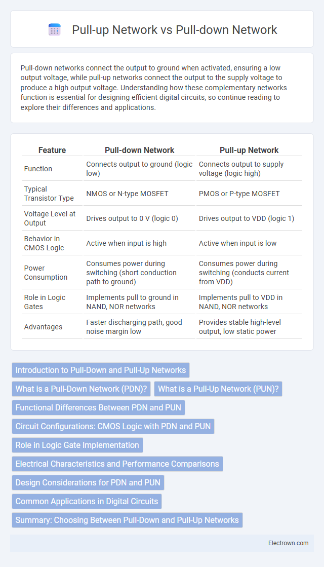
| Feature | Pull-down Network | Pull-up Network |
|---|---|---|
| Function | Connects output to ground (logic low) | Connects output to supply voltage (logic high) |
| Typical Transistor Type | NMOS or N-type MOSFET | PMOS or P-type MOSFET |
| Voltage Level at Output | Drives output to 0 V (logic 0) | Drives output to VDD (logic 1) |
| Behavior in CMOS Logic | Active when input is high | Active when input is low |
| Power Consumption | Consumes power during switching (short conduction path to ground) | Consumes power during switching (conducts current from VDD) |
| Role in Logic Gates | Implements pull to ground in NAND, NOR networks | Implements pull to VDD in NAND, NOR networks |
| Advantages | Faster discharging path, good noise margin low | Provides stable high-level output, low static power |
Introduction to Pull-Down and Pull-Up Networks
Pull-down and pull-up networks are fundamental components in CMOS digital circuits, responsible for driving output nodes to logic low and logic high states, respectively. The pull-up network typically consists of PMOS transistors connected to the positive supply voltage, while the pull-down network uses NMOS transistors connected to ground. These complementary configurations optimize power efficiency and switching speed in integrated circuit design.
What is a Pull-Down Network (PDN)?
A Pull-Down Network (PDN) is a circuit structure in digital logic that connects the output node to ground when a specific logic condition is met, primarily using NMOS transistors. This network ensures that the output is driven to a low voltage level, representing a logical "0," by providing a path to the negative supply terminal. Understanding the functionality of your PDN is crucial for designing efficient CMOS logic gates and minimizing power consumption in integrated circuits.
What is a Pull-Up Network (PUN)?
A Pull-Up Network (PUN) is a key component in CMOS logic circuits that connects the output to the positive supply voltage (VDD) when activated. It typically consists of PMOS transistors arranged to create a high output state, ensuring the output node is pulled up to VDD during certain logic conditions. Understanding your PUN's design is crucial for optimizing circuit speed, power consumption, and overall reliability in digital electronics.
Functional Differences Between PDN and PUN
The Pull-Down Network (PDN) consists of NMOS transistors that connect the output to ground, enabling the circuit to pull the output voltage down to a logic low level when activated. In contrast, the Pull-Up Network (PUN) comprises PMOS transistors that connect the output to the power supply voltage, driving the output to a logic high level. The functional difference lies in their complementary roles: PDN facilitates strong logic '0' output by conducting for true inputs, while PUN ensures a stable logic '1' output by conducting for false inputs, together forming a CMOS inverter or logic gate.
Circuit Configurations: CMOS Logic with PDN and PUN
CMOS logic circuits utilize both Pull-down Networks (PDN) and Pull-up Networks (PUN) to achieve efficient switching between logic states. The PDN, typically composed of NMOS transistors, connects the output node to the ground for logic LOW, while the PUN, formed by PMOS transistors, links the output to the supply voltage for logic HIGH. This complementary arrangement ensures low static power consumption and high noise margins in digital integrated circuits.
Role in Logic Gate Implementation
Pull-down and Pull-up networks play crucial roles in CMOS logic gate implementation by controlling the output voltage levels through transistor arrangements. The Pull-up network, typically composed of pMOS transistors, connects the output to the positive supply voltage (Vdd) when the logic gate output should be high. Conversely, the Pull-down network, made of nMOS transistors, connects the output to ground (GND) to drive the output low, ensuring efficient and complementary switching behavior essential for low power consumption and high noise margins.
Electrical Characteristics and Performance Comparisons
Pull-down networks typically use NMOS transistors to pull the output node to ground, offering low resistance and fast switching speeds but higher leakage currents compared to pull-up networks, which rely on PMOS transistors to connect the output to the supply voltage and demonstrate lower leakage with higher resistance and slower transitions. The electrical characteristics of pull-down networks enable better driving strength and quicker voltage discharge, enhancing performance in speed-critical applications, whereas pull-up networks provide better noise margins and stability but at the cost of slower rise times. Your circuit design must balance these trade-offs to optimize switching performance, power consumption, and signal integrity.
Design Considerations for PDN and PUN
Design considerations for Pull-down Networks (PDN) focus on minimizing resistance and capacitance to ensure fast discharge paths to ground, emphasizing NMOS transistor sizing and threshold voltage optimization. Pull-up Networks (PUN) require careful PMOS device sizing to balance drive strength and reduce static power consumption while maintaining stable output levels. Your design must account for complementary transistor behavior and parasitic effects to achieve efficient switching performance and low power usage.
Common Applications in Digital Circuits
Pull-down networks are widely used in NMOS logic circuits for applications requiring strong logic '0' output by connecting the output node to ground when activated. Pull-up networks, typically implemented using PMOS transistors, are essential in CMOS technology to pull the output node to the supply voltage, ensuring a strong logic '1' output. Both networks are critical in CMOS inverter design and complementary logic gates, enabling low power consumption and high-speed switching in digital circuits.
Summary: Choosing Between Pull-Down and Pull-Up Networks
Pull-down and pull-up networks are essential in digital circuit design, each providing distinct advantages depending on the required logic function and power efficiency. Pull-down networks use NMOS transistors to connect the output to ground when active, offering faster switching speeds and lower resistance paths, while pull-up networks employ PMOS transistors to link the output to the power supply, reducing power consumption in certain states. Your choice between these networks should consider factors such as device speed, power requirements, and overall circuit complexity to optimize performance and efficiency.
Pull-down vs Pull-up Network Infographic