The ground plane provides a stable reference voltage and reduces electromagnetic interference, while the signal plane carries the actual data or control signals in a circuit. Understanding the differences and roles of ground and signal planes is crucial for optimizing your PCB design; read on to explore their specific impacts.
Table of Comparison
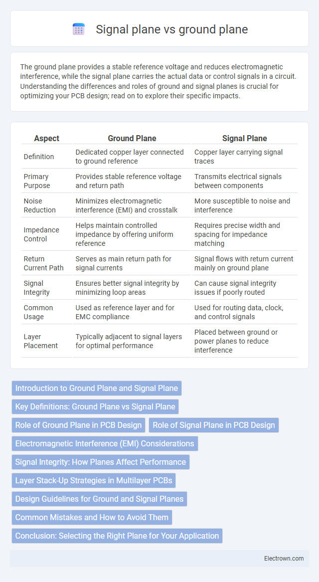
| Aspect | Ground Plane | Signal Plane |
|---|---|---|
| Definition | Dedicated copper layer connected to ground reference | Copper layer carrying signal traces |
| Primary Purpose | Provides stable reference voltage and return path | Transmits electrical signals between components |
| Noise Reduction | Minimizes electromagnetic interference (EMI) and crosstalk | More susceptible to noise and interference |
| Impedance Control | Helps maintain controlled impedance by offering uniform reference | Requires precise width and spacing for impedance matching |
| Return Current Path | Serves as main return path for signal currents | Signal flows with return current mainly on ground plane |
| Signal Integrity | Ensures better signal integrity by minimizing loop areas | Can cause signal integrity issues if poorly routed |
| Common Usage | Used as reference layer and for EMC compliance | Used for routing data, clock, and control signals |
| Layer Placement | Typically adjacent to signal layers for optimal performance | Placed between ground or power planes to reduce interference |
Introduction to Ground Plane and Signal Plane
Ground planes serve as a continuous reference point for electrical signals, providing a low-impedance path that minimizes noise and electromagnetic interference in circuit designs. Signal planes, on the other hand, carry the actual data or power signals and require careful routing to avoid crosstalk and maintain signal integrity. Understanding the distinction between ground plane and signal plane is essential for optimizing your PCB layout and enhancing overall performance.
Key Definitions: Ground Plane vs Signal Plane
A ground plane is a continuous conductive layer that serves as a reference voltage level and helps minimize electromagnetic interference by providing a low-impedance path to ground. A signal plane, in contrast, carries the electrical signals between components and is designed to ensure signal integrity by controlling impedance and reducing crosstalk. In high-speed PCB design, maintaining clear separation between ground and signal planes is crucial for effective noise reduction and signal transmission.
Role of Ground Plane in PCB Design
The ground plane in PCB design serves as a low-impedance return path for electrical signals, minimizing noise and electromagnetic interference (EMI). It stabilizes voltage levels across the board, improving signal integrity and reducing the risk of ground loops. Your PCB's performance and reliability depend heavily on an effective ground plane layout to ensure proper grounding and signal reference.
Role of Signal Plane in PCB Design
The signal plane in PCB design is responsible for routing electrical signals between components, ensuring efficient and accurate data transmission. It plays a crucial role in maintaining signal integrity by minimizing noise and crosstalk through controlled impedance and proper trace layout. Unlike the ground plane, which provides a return path and reduces electromagnetic interference, the signal plane must be carefully planned to optimize circuit performance and reliability.
Electromagnetic Interference (EMI) Considerations
A continuous ground plane in PCB design significantly reduces electromagnetic interference (EMI) by providing a low-impedance return path and minimizing loop area for high-frequency signals. Signal planes adjacent to ground planes improve signal integrity by confining electromagnetic fields and reducing crosstalk. Proper stacking with ground and signal layers also helps control impedance and prevents EMI emission and susceptibility.
Signal Integrity: How Planes Affect Performance
Ground planes provide a low-impedance return path that minimizes electromagnetic interference and crosstalk, significantly enhancing signal integrity. Signal planes, when properly layered with ground planes, reduce noise coupling and maintain consistent impedance, crucial for high-speed data transmission. Your PCB design benefits from optimized ground and signal plane arrangements by ensuring cleaner signals and reduced signal degradation.
Layer Stack-Up Strategies in Multilayer PCBs
Layer stack-up strategies in multilayer PCBs prioritize positioning the ground plane adjacent to signal layers to minimize impedance and reduce electromagnetic interference (EMI). A solid ground plane provides a low-inductance return path, enhancing signal integrity by maintaining controlled impedance and reducing crosstalk in high-speed designs. Optimal stack-ups typically alternate signal and ground planes, ensuring effective signal referencing and minimizing loop areas for high-frequency signals.
Design Guidelines for Ground and Signal Planes
Designing effective ground and signal planes requires maintaining low impedance paths to minimize noise and ensure signal integrity. Your PCB layout should separate ground and signal planes with a consistent dielectric layer to reduce electromagnetic interference (EMI) and crosstalk. Ensuring continuous ground planes beneath signal traces provides controlled impedance and enhances overall system performance.
Common Mistakes and How to Avoid Them
Common mistakes in PCB design often include mixing the ground plane with the signal plane, leading to increased noise and signal interference due to improper return current paths. Avoid these issues by maintaining a continuous, uninterrupted ground plane separate from signal layers, ensuring controlled impedance and minimizing ground loops. Your design integrity benefits significantly from strategic layout planning that prioritizes dedicated signal and ground planes for effective electromagnetic compatibility and signal integrity.
Conclusion: Selecting the Right Plane for Your Application
Choosing between a ground plane and a signal plane requires careful consideration of your circuit's electromagnetic compatibility and noise reduction needs. Ground planes excel at providing a stable reference and minimizing electromagnetic interference, making them ideal for high-frequency or sensitive analog designs. Signal planes offer flexible routing options but may introduce noise and crosstalk, so they are best suited for lower-speed digital circuits or when PCB layer constraints exist.
Ground plane vs signal plane Infographic