Clock gating reduces power consumption by disabling the clock signal to inactive circuits, minimizing switching activity, while power gating cuts off the power supply to idle blocks, eliminating leakage current entirely. Understanding these techniques can help you optimize energy efficiency in your designs; discover more about their applications and benefits in the rest of the article.
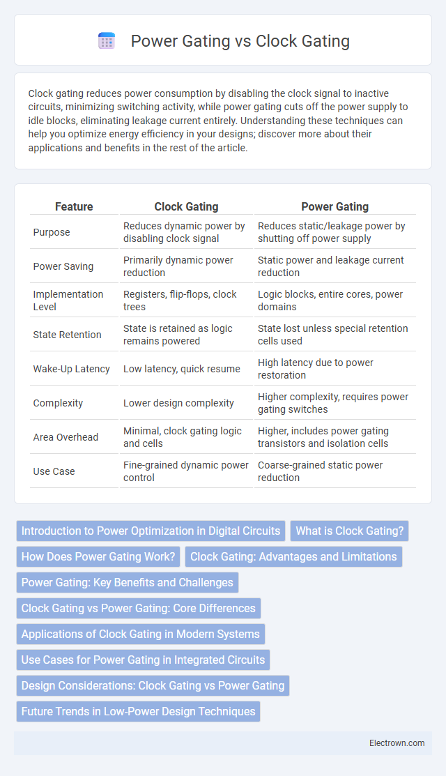
Table of Comparison
| Feature | Clock Gating | Power Gating |
|---|---|---|
| Purpose | Reduces dynamic power by disabling clock signal | Reduces static/leakage power by shutting off power supply |
| Power Saving | Primarily dynamic power reduction | Static power and leakage current reduction |
| Implementation Level | Registers, flip-flops, clock trees | Logic blocks, entire cores, power domains |
| State Retention | State is retained as logic remains powered | State lost unless special retention cells used |
| Wake-Up Latency | Low latency, quick resume | High latency due to power restoration |
| Complexity | Lower design complexity | Higher complexity, requires power gating switches |
| Area Overhead | Minimal, clock gating logic and cells | Higher, includes power gating transistors and isolation cells |
| Use Case | Fine-grained dynamic power control | Coarse-grained static power reduction |
Introduction to Power Optimization in Digital Circuits
Power optimization in digital circuits involves techniques like Clock Gating and Power Gating to reduce energy consumption and improve efficiency. Clock Gating minimizes dynamic power by disabling the clock signal to inactive circuit blocks, while Power Gating reduces static power by cutting off the power supply to idle modules. Understanding these methods enhances your ability to design low-power integrated circuits essential for battery-operated and high-performance applications.
What is Clock Gating?
Clock gating is a power-saving technique in digital circuits that disables the clock signal to idle functional units, effectively reducing dynamic power consumption by preventing unnecessary switching activity. It operates by inserting gating logic, such as AND or OR gates, to control clock propagation based on enable signals. Widely used in ASIC and FPGA designs, clock gating optimizes energy efficiency without disrupting the circuit's overall timing or functionality.
How Does Power Gating Work?
Power gating works by disconnecting the power supply to idle circuit blocks using sleep transistors, effectively cutting off leakage current and reducing static power consumption. When a circuit is inactive, power gating switches off the power at the transistors, placing the block in a low-power state without losing data stored in retention cells. This technique complements clock gating by targeting leakage power, significantly enhancing energy efficiency in integrated circuits.
Clock Gating: Advantages and Limitations
Clock gating reduces dynamic power consumption by disabling the clock signal to inactive circuit blocks, resulting in lower switching activity and improved energy efficiency. It offers fine-grained control with minimal impact on performance and area overhead but cannot eliminate leakage power, making it less effective for static power reduction. Limitations include increased design complexity due to clock tree modifications and potential clock skew issues that require careful timing analysis.
Power Gating: Key Benefits and Challenges
Power gating significantly reduces leakage power by completely shutting off current to inactive blocks, enhancing overall energy efficiency in integrated circuits. Its key benefits include prolonged battery life in portable devices and reduced thermal output in high-performance systems. Challenges lie in managing wake-up latency and ensuring reliable state retention during power-off periods, which require careful design and control circuitry.
Clock Gating vs Power Gating: Core Differences
Clock gating reduces dynamic power consumption by disabling the clock signal to idle circuits, effectively stopping unnecessary switching activity. Power gating cuts off the power supply to inactive blocks, eliminating leakage power and achieving greater energy savings during long idle periods. Understanding these core differences helps you choose the optimal strategy for power management in your digital designs.
Applications of Clock Gating in Modern Systems
Clock gating is primarily used in digital circuits to reduce dynamic power consumption by disabling the clock signal to inactive modules, improving energy efficiency in processors and SoCs. It is widely applied in mobile devices, embedded systems, and high-performance computing to extend battery life and manage thermal output during idle or low-activity periods. Your modern system benefits from clock gating by maintaining performance while minimizing power usage in components like CPUs, GPUs, and memory interfaces.
Use Cases for Power Gating in Integrated Circuits
Power gating in integrated circuits is primarily used to reduce leakage power by completely shutting off the power supply to inactive blocks during low activity periods, making it ideal for battery-powered and energy-sensitive devices. This technique is commonly employed in smartphones, laptops, and IoT devices to extend battery life and improve thermal management. You benefit from enhanced overall energy efficiency and prolonged device longevity when power gating is applied effectively in your circuit design.
Design Considerations: Clock Gating vs Power Gating
Design considerations for clock gating focus on reducing dynamic power by disabling the clock signal to inactive modules, enabling fine-grained control with minimal impact on data retention and wake-up latency. Power gating targets leakage power reduction by cutting off the power supply to idle circuits, requiring careful management of state retention and potential wake-up delays, making it ideal for longer idle periods. Your choice between clock gating and power gating depends on the balance between power savings, design complexity, and system performance requirements.
Future Trends in Low-Power Design Techniques
Future trends in low-power design techniques emphasize the integration of clock gating and power gating to achieve enhanced energy efficiency in semiconductor devices. Advanced clock gating methods focus on fine-grained control and machine learning algorithms to dynamically minimize clock distribution power, while power gating evolves with adaptive power domains and retention strategies to reduce leakage currents during idle states. Emerging technologies such as multi-threshold CMOS (MTCMOS) and body biasing are expected to synergize with these gating techniques, pushing the boundaries of ultra-low-power applications in IoT, mobile, and AI-driven systems.
Clock Gating vs Power Gating Infographic