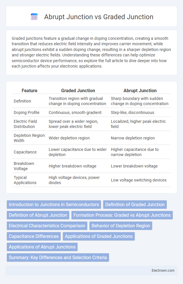
Graded junctions feature a gradual change in doping concentration, creating a smooth transition that reduces electric field intensity and improves carrier movement, while abrupt junctions exhibit a sudden doping change, resulting in a sharper depletion region and stronger electric fields. Understanding these differences can help optimize semiconductor device performance, so explore the full article to dive deeper into how each junction affects your electronic applications.
Table of Comparison
| Feature | Graded Junction | Abrupt Junction |
|---|---|---|
| Definition | Transition region with gradual change in doping concentration | Sharp boundary with sudden change in doping concentration |
| Doping Profile | Continuous, smooth gradient | Step-like, discontinuous |
| Electric Field Distribution | Spread over a wider region, lower peak electric field | Localized, higher peak electric field |
| Depletion Region Width | Wider depletion region | Narrow depletion region |
| Capacitance | Lower capacitance due to wider depletion | Higher capacitance due to narrow depletion |
| Breakdown Voltage | Higher breakdown voltage | Lower breakdown voltage |
| Typical Applications | High voltage devices, power diodes | Low voltage switching devices |
Introduction to Junctions in Semiconductors
Junctions in semiconductors form the critical boundary between p-type and n-type materials, enabling the control of charge carrier flow essential for device operation. A graded junction features a gradual transition of doping concentration, minimizing electric field spikes and improving carrier mobility. In contrast, an abrupt junction has a sudden change in doping levels, producing a sharp depletion region that enhances rectifying behavior but can increase electric field intensity.
Definition of Graded Junction
A graded junction is a semiconductor interface where the transition between p-type and n-type materials occurs gradually through a continuous change in doping concentration. This gradual variation reduces electric field spikes and improves device performance by minimizing carrier recombination and enhancing charge separation. Unlike abrupt junctions, graded junctions offer smoother band bending, which benefits devices sensitive to electric field distribution, such as solar cells and transistors.
Definition of Abrupt Junction
An abrupt junction refers to a sharp transition between p-type and n-type semiconductor regions where the doping concentration changes suddenly at the junction interface. This results in a distinct depletion region with well-defined electrical characteristics and a narrow transition zone. Your semiconductor device performance can be influenced by the choice between an abrupt junction and a graded junction, affecting parameters like capacitance and breakdown voltage.
Formation Process: Graded vs Abrupt Junctions
Graded junctions form through a gradual change in doping concentration, resulting in a smooth transition between p-type and n-type materials, whereas abrupt junctions have a sharp, immediate change in doping levels at the interface. The formation process of graded junctions often involves controlled diffusion techniques to achieve the gradual doping gradient, while abrupt junctions are typically created using rapid doping or ion implantation methods. Understanding your device's application helps determine whether a graded or abrupt junction offers better performance based on the formation process and electrical characteristics.
Electrical Characteristics Comparison
Graded junctions exhibit a gradual change in doping concentration, resulting in lower peak electric fields and reduced junction capacitance compared to abrupt junctions, which have a sudden doping change causing high electric fields and increased capacitance. The smoother transition in graded junctions enhances charge carrier mobility and reduces leakage currents, improving device reliability under high voltage stress. Abrupt junctions, however, offer faster switching speeds due to their sharper depletion region boundaries, making them suitable for high-frequency applications despite higher electric field stress.
Behavior of Depletion Region
The depletion region in a graded junction varies gradually due to the smooth transition of doping concentration, resulting in a wider and less abrupt boundary compared to an abrupt junction where the depletion region is sharply defined with an abrupt change in doping levels. This gradual change in the graded junction leads to a varying electric field across the depletion region, whereas in the abrupt junction the electric field is more uniform and concentrated. Understanding this behavior is crucial for optimizing your semiconductor device performance in applications requiring precise control over charge carrier dynamics.
Capacitance Differences
Graded junctions exhibit lower junction capacitance compared to abrupt junctions due to their gradual doping profile, which reduces charge storage at the depletion region. In contrast, abrupt junctions have a steeper doping gradient, resulting in higher capacitance and faster charge accumulation. Understanding these capacitance differences helps optimize your semiconductor device's switching speed and frequency response.
Applications of Graded Junctions
Graded junctions are widely used in semiconductor devices where smooth transition of dopant concentration improves the electric field distribution, such as in varactor diodes and bipolar junction transistors (BJTs) to enhance frequency response and reduce noise. These junctions facilitate better control of depletion region width, making them ideal for high-frequency and analog applications where abrupt junctions might cause performance degradation. The gradual change in doping concentration supports improved breakdown voltage characteristics and minimizes carrier recombination, which is crucial in power devices and photodetectors.
Applications of Abrupt Junctions
Abrupt junctions are predominantly used in high-speed switching devices and digital integrated circuits due to their sharp boundary between the p-type and n-type regions, which allows for faster carrier transition and lower capacitance. These junctions are essential in applications such as diodes, transistors, and photodetectors where precise control of charge carriers is required to enhance device performance. The abrupt change in doping concentration enables efficient operation in rectifiers, logic gates, and high-frequency electronic components.
Summary: Key Differences and Selection Criteria
Graded junctions feature a gradual transition in doping concentration, resulting in reduced electric field spikes and enhanced carrier mobility compared to abrupt junctions, which have an immediate dopant concentration change causing stronger electric fields and higher junction capacitance. Selection criteria depend on device requirements: graded junctions are preferred for high-performance analog components needing smooth electrical characteristics, while abrupt junctions suit digital applications demanding sharp switching behavior. Material compatibility, fabrication complexity, and intended operating frequency also influence the choice between graded and abrupt junctions.
Graded Junction vs Abrupt Junction Infographic