Fully Depleted SOI offers improved performance and lower power consumption by eliminating the floating body effect, while Partially Depleted SOI retains some floating body phenomena due to thicker silicon films. Discover how these differences impact your device design and optimize semiconductor efficiency by reading the full article.
Table of Comparison
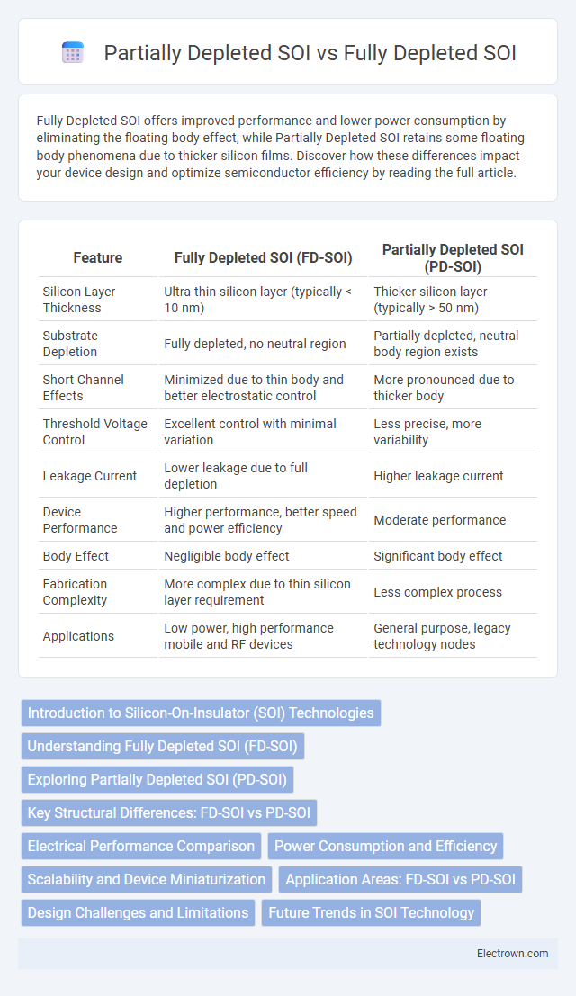
| Feature | Fully Depleted SOI (FD-SOI) | Partially Depleted SOI (PD-SOI) |
|---|---|---|
| Silicon Layer Thickness | Ultra-thin silicon layer (typically < 10 nm) | Thicker silicon layer (typically > 50 nm) |
| Substrate Depletion | Fully depleted, no neutral region | Partially depleted, neutral body region exists |
| Short Channel Effects | Minimized due to thin body and better electrostatic control | More pronounced due to thicker body |
| Threshold Voltage Control | Excellent control with minimal variation | Less precise, more variability |
| Leakage Current | Lower leakage due to full depletion | Higher leakage current |
| Device Performance | Higher performance, better speed and power efficiency | Moderate performance |
| Body Effect | Negligible body effect | Significant body effect |
| Fabrication Complexity | More complex due to thin silicon layer requirement | Less complex process |
| Applications | Low power, high performance mobile and RF devices | General purpose, legacy technology nodes |
Introduction to Silicon-On-Insulator (SOI) Technologies
Silicon-On-Insulator (SOI) technologies utilize a layered silicon-insulator-silicon substrate to enhance transistor performance by reducing parasitic capacitance and leakage currents. Fully Depleted SOI (FD-SOI) features an ultra-thin silicon film on the insulator, enabling better control of the channel and offering reduced short-channel effects compared to Partially Depleted SOI (PD-SOI), which has a thicker silicon layer leading to partial depletion of the channel. These structural differences make FD-SOI ideal for low-power, high-performance applications, while PD-SOI is often used where cost and legacy compatibility are prioritized.
Understanding Fully Depleted SOI (FD-SOI)
Fully Depleted SOI (FD-SOI) technology utilizes an ultra-thin silicon layer on an insulator, allowing better control of the transistor channel and reducing leakage currents compared to Partially Depleted SOI (PD-SOI). This leads to improved power efficiency, higher performance, and enhanced scaling capabilities, making FD-SOI ideal for advanced low-power applications. You can leverage FD-SOI to achieve superior device reliability and energy savings in modern semiconductor designs.
Exploring Partially Depleted SOI (PD-SOI)
Partially Depleted SOI (PD-SOI) technology features a thin silicon film over an insulating layer, creating a partially depleted channel that offers improved speed and scalability compared to bulk silicon. PD-SOI provides moderate power efficiency and reduced parasitic capacitance, benefiting applications requiring a balance between performance and power consumption. You can leverage PD-SOI for enhanced device robustness and cost-effective manufacturing in a variety of semiconductor designs.
Key Structural Differences: FD-SOI vs PD-SOI
Fully Depleted Silicon-On-Insulator (FD-SOI) features an ultra-thin silicon layer, typically less than 10 nm, allowing the channel to be fully depleted of carriers, which significantly reduces short-channel effects and improves electrostatic control. In contrast, Partially Depleted SOI (PD-SOI) utilizes a thicker silicon layer where the channel remains partially depleted, resulting in a floating body effect that can cause variability in device performance. The buried oxide (BOX) thickness in FD-SOI is optimized to balance capacitance and leakage, while PD-SOI commonly has a thicker BOX that isolates the body but limits electrostatic control efficiency.
Electrical Performance Comparison
Fully Depleted SOI (FD-SOI) offers superior electrical performance compared to Partially Depleted SOI (PD-SOI) due to reduced short-channel effects and lower leakage currents. Your device benefits from enhanced threshold voltage control and improved subthreshold slope in FD-SOI technology, resulting in higher speed and energy efficiency. PD-SOI, while simpler to manufacture, typically exhibits increased parasitic capacitance and less effective electrostatic control, limiting its performance in advanced low-power applications.
Power Consumption and Efficiency
Fully Depleted Silicon-On-Insulator (FD-SOI) technology offers significantly lower power consumption compared to Partially Depleted SOI (PD-SOI) due to its ultra-thin silicon layer, which reduces leakage currents and enhances electrostatic control. FD-SOI devices achieve higher energy efficiency by enabling dynamic threshold voltage modulation, contributing to better performance-per-watt in low-power and high-speed applications. PD-SOI lacks this fine control, resulting in higher static power dissipation and less optimal efficiency under varying operational conditions.
Scalability and Device Miniaturization
Fully Depleted Silicon-On-Insulator (FD-SOI) offers superior scalability and device miniaturization compared to Partially Depleted SOI (PD-SOI) due to its ultra-thin silicon layer that reduces short-channel effects and enhances electrostatic control. FD-SOI enables smaller transistor dimensions and lower power consumption while maintaining performance, making it ideal for advanced nodes below 28nm. You benefit from FD-SOI's ability to support aggressive device scaling while minimizing variability and leakage currents in nanoscale semiconductor manufacturing.
Application Areas: FD-SOI vs PD-SOI
FD-SOI technology is widely used in low-power and high-performance applications such as mobile devices, automotive electronics, and IoT sensors due to its superior control over short-channel effects and reduced leakage currents. PD-SOI remains suitable for legacy RF and mixed-signal circuits where cost efficiency and established design flows are prioritized, though it exhibits higher power consumption and less scalability. The choice between FD-SOI and PD-SOI depends on application requirements for power efficiency, integration complexity, and frequency performance.
Design Challenges and Limitations
Fully Depleted SOI (FD-SOI) faces design challenges such as stringent control of silicon film thickness and buried oxide uniformity to prevent short-channel effects and ensure electrostatic integrity. Partially Depleted SOI (PD-SOI) suffers from floating body effects that cause threshold voltage variability and hysteresis, complicating device reliability and stability. Both technologies struggle with self-heating issues due to the buried oxide layer, impacting performance and necessitating careful thermal management in circuit design.
Future Trends in SOI Technology
Future trends in SOI technology emphasize the advancement of Fully Depleted SOI (FD-SOI) due to its superior electrostatic control and reduced power consumption compared to Partially Depleted SOI (PD-SOI). Industry momentum favors FD-SOI for its enhanced scalability and performance in low-power and high-frequency applications, making it a key enabler for next-generation IoT and 5G devices. Your designs can benefit from these innovations as FD-SOI continues to drive customizability and energy efficiency in emerging semiconductor solutions.
Fully Depleted SOI vs Partially Depleted SOI Infographic