Metal 1 and Metal 2 layers differ primarily in their role within integrated circuit design, where Metal 1 is typically used for local interconnections and Metal 2 for longer, more complex routing paths. Understanding these distinctions can optimize your chip's performance and layout efficiency, so continue reading to explore the specific characteristics and applications of Metal 1 versus Metal 2 routing.
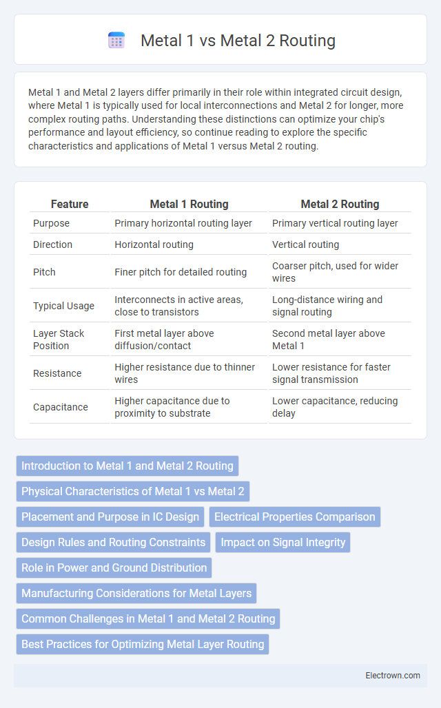
Table of Comparison
| Feature | Metal 1 Routing | Metal 2 Routing |
|---|---|---|
| Purpose | Primary horizontal routing layer | Primary vertical routing layer |
| Direction | Horizontal routing | Vertical routing |
| Pitch | Finer pitch for detailed routing | Coarser pitch, used for wider wires |
| Typical Usage | Interconnects in active areas, close to transistors | Long-distance wiring and signal routing |
| Layer Stack Position | First metal layer above diffusion/contact | Second metal layer above Metal 1 |
| Resistance | Higher resistance due to thinner wires | Lower resistance for faster signal transmission |
| Capacitance | Higher capacitance due to proximity to substrate | Lower capacitance, reducing delay |
Introduction to Metal 1 and Metal 2 Routing
Metal 1 and Metal 2 routing are layers in integrated circuit design used to connect various components on a chip. Metal 1 routing typically serves as the primary horizontal interconnect layer, while Metal 2 routing is oriented vertically to facilitate crossing wires without interference. Understanding the roles of Metal 1 and Metal 2 routing helps optimize your chip layout for improved signal integrity and minimized crosstalk.
Physical Characteristics of Metal 1 vs Metal 2
Metal 1 typically has narrower width and pitch compared to Metal 2, enabling finer routing and higher density interconnects near the transistor level. Metal 2 usually features increased thickness and wider spacing to reduce resistance and support longer-distance signal transmission across the chip. These physical differences optimize Metal 1 for local connectivity and Metal 2 for global routing, balancing performance and reliability in integrated circuit design.
Placement and Purpose in IC Design
Metal 1 routing in IC design primarily handles local interconnections between transistors within a standard cell, ensuring precise placement for efficient signal transmission at the transistor level. Metal 2 routing serves as an intermediate layer, connecting multiple Metal 1 routes and facilitating communication across larger sections of the chip. Your design's performance and area optimization depend on strategically balancing Metal 1's fine-grain placement with Metal 2's broader routing capabilities.
Electrical Properties Comparison
Metal 1 offers lower resistance due to its wider linewidth and thicker deposition, enhancing signal integrity and reducing RC delay compared to Metal 2. Metal 2, while thinner and narrower, provides better capacitive coupling control, minimizing crosstalk in dense routing layers. The trade-off between resistance and capacitance in Metal 1 versus Metal 2 significantly impacts high-frequency performance and power distribution efficiency within integrated circuits.
Design Rules and Routing Constraints
Metal 1 and Metal 2 routing layers have distinct design rules critical for maintaining signal integrity and manufacturability. Metal 1 typically requires tighter spacing and narrower widths due to its proximity to the transistor layer, imposing stricter routing constraints to avoid shorts and ensure proper connectivity. Metal 2, situated above Metal 1, allows for wider traces and larger spacing, facilitating longer and less complex routing paths while reducing parasitic capacitance and crosstalk.
Impact on Signal Integrity
Metal 1 routing, being the closest layer to the substrate, often experiences higher parasitic capacitance and crosstalk, which can degrade signal integrity in high-frequency circuits. Metal 2 routing, positioned above Metal 1, generally offers lower parasitic coupling and better shielding, resulting in improved signal integrity and reduced electromagnetic interference. Optimizing routing by choosing Metal 2 for critical high-speed signals enhances overall circuit performance by minimizing signal loss and timing errors.
Role in Power and Ground Distribution
Metal 1 and Metal 2 layers serve distinct roles in power and ground distribution within integrated circuits. Metal 1 is typically used for fine routing and local interconnects, while Metal 2 provides wider, lower-resistance paths that efficiently distribute power and ground signals across larger chip areas. Optimizing your design by leveraging Metal 2 for power and ground grids enhances current handling and reduces voltage drop, improving overall circuit reliability.
Manufacturing Considerations for Metal Layers
Metal 1 and Metal 2 routing differ significantly in manufacturing considerations due to their placement and function within semiconductor devices. Metal 1, being the first metal layer, is typically used for local interconnects and requires fine pitch and high precision lithography to minimize resistance and capacitance, directly impacting device performance. Metal 2, positioned above Metal 1, often serves as a higher-level routing layer, allowing for wider traces and relaxed spacing because it is less constrained by transistor proximity and can incorporate advanced planarization and deposition techniques to enhance overall circuit reliability.
Common Challenges in Metal 1 and Metal 2 Routing
Metal 1 routing often faces challenges related to congestion due to its proximity to standard cells and limited track availability, which can hinder signal integrity and routing efficiency. Metal 2 routing, while offering more routing flexibility and less congestion than Metal 1, encounters issues such as increased resistance and capacitance leading to potential delay and crosstalk. Addressing these common challenges in Metal 1 and Metal 2 routing is essential for optimizing your integrated circuit performance and ensuring reliable signal transmission.
Best Practices for Optimizing Metal Layer Routing
Optimizing Metal 1 and Metal 2 routing involves prioritizing Metal 1 for local, fine-pitched connections due to its proximity to the transistor layer, while using Metal 2 for longer, higher-capacity signal routing to reduce congestion. Best practices include maintaining consistent wire spacing to minimize crosstalk, enforcing design rules for via placement to ensure reliable inter-layer connectivity, and using parallel routing on Metal 1 with perpendicular routing on Metal 2 to simplify layout and improve signal integrity. Effective layer assignment and careful planning of metal density across both layers are critical for optimizing performance and manufacturability in advanced integrated circuits.
Metal 1 vs Metal 2 Routing Infographic