Deep N-Well technology enhances isolation and reduces substrate noise, improving performance in mixed-signal integrated circuits, while Shallow N-Well offers benefits in planar area efficiency and faster transistor switching speeds. Discover how these differences impact your semiconductor design choices in the full article.
Table of Comparison
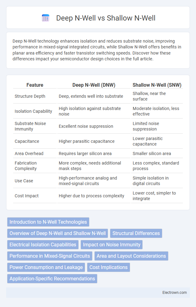
| Feature | Deep N-Well (DNW) | Shallow N-Well (SNW) |
|---|---|---|
| Structure Depth | Deep, extends well into substrate | Shallow, near the surface |
| Isolation Capability | High isolation against substrate noise | Moderate isolation, less effective |
| Substrate Noise Immunity | Excellent noise suppression | Limited noise suppression |
| Capacitance | Higher parasitic capacitance | Lower parasitic capacitance |
| Area Overhead | Requires larger silicon area | Smaller silicon area |
| Fabrication Complexity | More complex, needs additional mask steps | Less complex, standard process |
| Use Case | High-performance analog and mixed-signal circuits | Simple isolation in digital circuits |
| Cost Impact | Higher due to process complexity | Lower cost, simpler to integrate |
Introduction to N-Well Technologies
N-Well technologies form the foundation of CMOS integrated circuit design, differentiating primarily into Deep N-Well and Shallow N-Well structures based on doping depth and electrical isolation properties. Deep N-Well provides enhanced isolation by embedding a thicker n-type region, improving latch-up immunity and reducing substrate noise in mixed-signal and RF applications. Shallow N-Well features a thinner n-type layer, suitable for standard CMOS logic circuits where minimal area and simpler processing are prioritized over isolation performance.
Overview of Deep N-Well and Shallow N-Well
Deep N-Well (DNW) and Shallow N-Well (SNW) are critical structures in CMOS technology for isolating and protecting transistors in integrated circuits. DNW extends deeper into the substrate, providing enhanced isolation and reducing parasitic capacitance, making it ideal for high-voltage applications and mixed-signal designs. SNW, confined closer to the surface, offers sufficient isolation for low-voltage digital circuits and supports higher transistor density with simpler fabrication.
Structural Differences
Deep N-Well structures extend further into the silicon substrate compared to Shallow N-Well, providing better isolation and reduced parasitic capacitance. Shallow N-Wells are confined closer to the surface, offering faster switching speeds but less noise immunity. Your choice between Deep and Shallow N-Well depends on the required balance between device isolation and speed in integrated circuit design.
Electrical Isolation Capabilities
Deep N-Well technology offers superior electrical isolation capabilities by extending deeper into the silicon substrate, effectively reducing substrate noise coupling and latch-up susceptibility compared to Shallow N-Well structures. Shallow N-Well provides limited isolation primarily near the surface, making it less effective in high-voltage or mixed-signal applications where robust noise isolation is critical. Enhanced isolation in Deep N-Well designs improves overall circuit stability and performance in densely integrated CMOS processes.
Impact on Noise Immunity
Deep N-Well structures offer superior noise immunity compared to shallow N-Well designs by providing enhanced isolation between circuit components, which reduces substrate noise coupling. The increased depth of Deep N-Wells effectively shields sensitive analog and mixed-signal circuits from digital switching noise, improving overall signal integrity. Your choice between Deep and Shallow N-Well can significantly influence the robustness of noise-sensitive applications in integrated circuits.
Performance in Mixed-Signal Circuits
Deep N-Well structures provide enhanced isolation and reduced substrate noise coupling in mixed-signal circuits, improving analog performance and minimizing digital interference. Shallow N-Well offers lower parasitic capacitance but is less effective in isolating sensitive analog components from noisy digital substrates. Optimizing performance in mixed-signal designs requires leveraging Deep N-Well for superior noise immunity while balancing area and process complexity.
Area and Layout Considerations
Deep N-Well structures require more silicon area compared to Shallow N-Well due to their increased depth and complexity, impacting overall chip size and cost. Layout considerations for Deep N-Well involve careful isolation management and junction placement to minimize parasitic effects, whereas Shallow N-Well enables more compact designs with simpler isolation requirements. Your design choice influences routing density and thermal characteristics, making area optimization crucial in high-density integrated circuits.
Power Consumption and Leakage
Deep N-Well technology significantly reduces substrate noise coupling and improves isolation, leading to lower power consumption in mixed-signal and RF circuits compared to Shallow N-Well structures. Leakage currents are minimized in Deep N-Well due to its enhanced diffusion depth, which effectively suppresses parasitic leakage paths, resulting in better overall leakage control. In contrast, Shallow N-Well designs typically exhibit higher leakage and power dissipation, limiting their suitability for low-power applications.
Cost Implications
Deep N-Well structures generally incur higher fabrication costs due to more complex implantation and diffusion processes compared to Shallow N-Well designs. The increased process steps and thicker epitaxial layers required for Deep N-Wells lead to longer manufacturing times and higher material consumption. Shallow N-Well solutions offer cost advantages by simplifying wafer processing and enabling higher yield in standard CMOS technology nodes.
Application-Specific Recommendations
Deep N-Well structures are preferred in high-voltage and mixed-signal IC applications due to their enhanced isolation capabilities and reduced substrate noise coupling. Shallow N-Well is more suitable for low-voltage digital circuits where faster switching speeds and lower parasitic capacitance are critical. Application-specific recommendations highlight Deep N-Well for analog/mixed-signal designs requiring robust noise immunity, whereas Shallow N-Well optimizes performance in dense digital logic environments.
Deep N-Well vs Shallow N-Well Infographic