Schematic Driven Layout (SDL) focuses on creating a layout directly from the schematic, ensuring seamless synchronization between design intent and physical implementation, whereas Layout Driven Schematic (LDS) starts with the layout to generate or adjust the schematic, optimizing for physical constraints. Understanding the differences between these methods can enhance Your design workflow; explore the article to discover which approach best suits your project needs.
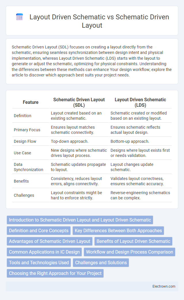
Table of Comparison
| Feature | Schematic Driven Layout (SDL) | Layout Driven Schematic (LDS) |
|---|---|---|
| Definition | Layout created based on an existing schematic. | Schematic created or modified based on an existing layout. |
| Primary Focus | Ensures layout matches schematic connectivity. | Ensures schematic reflects actual layout design. |
| Design Flow | Top-down approach. | Bottom-up approach. |
| Use Case | New designs where schematic drives layout process. | Designs where layout exists first or needs validation. |
| Data Synchronization | Schematic updates propagate to layout. | Layout changes update schematic. |
| Benefits | Consistency, reduces layout errors, aligns connectivity. | Validates layout correctness, ensures schematic accuracy. |
| Challenges | Layout constraints might be hard to enforce strictly. | Reverse-engineering schematics can be complex. |
Introduction to Schematic Driven Layout and Layout Driven Schematic
Schematic Driven Layout (SDL) prioritizes creating the electrical schematic first, which serves as a blueprint for designing the physical layout, ensuring circuit functionality aligns with design intent. Layout Driven Schematic (LDS) begins with the physical layout design, from which the schematic is then generated or updated, facilitating backward verification and detail refinement. SDL is commonly used for initial design clarity, while LDS enhances post-layout adjustments and iterative improvements.
Definition and Core Concepts
Schematic Driven Layout involves creating a physical design based directly on a predefined circuit schematic, ensuring the physical layout accurately reflects the electrical connections and component placements specified. Layout Driven Schematic, conversely, starts with the physical layout to generate or modify the circuit schematic, emphasizing real-world constraints and design adjustments during the schematic creation process. Understanding these core concepts helps you streamline design accuracy and maintain synchronization between schematic and layout in electronic design automation (EDA).
Key Differences Between Both Approaches
Schematic Driven Layout prioritizes the creation of a detailed circuit schematic before the physical layout, ensuring design intent and connectivity are accurately defined upfront. Layout Driven Schematic begins with the physical placement of components on the PCB, allowing the schematic to evolve based on spatial constraints and real-world implementation. Your choice depends on workflow preferences: Schematic Driven Layout offers a top-down approach emphasizing logical design, while Layout Driven Schematic provides a bottom-up process focusing on physical optimization.
Advantages of Schematic Driven Layout
Schematic Driven Layout offers precise synchronization between the circuit design and physical layout, reducing errors and improving design accuracy. This approach enhances efficiency by automatically updating the layout to reflect schematic changes, minimizing manual adjustments and saving time. Your workflow benefits from streamlined verification processes and better adherence to design rules, ensuring seamless integration between design intent and physical implementation.
Benefits of Layout Driven Schematic
Layout Driven Schematic (LDS) integrates physical layout information early into the schematic design process, improving design accuracy and reducing errors by reflecting real-world constraints. This approach enhances electrical verification and timing closure by ensuring that parasitics and routing complexities are accounted for upfront, leading to more reliable circuit performance. Your designs benefit from streamlined iterations and faster convergence, boosting overall productivity and reducing costly redesigns.
Common Applications in IC Design
Schematic Driven Layout is commonly used in analog and mixed-signal IC design to ensure accurate device matching and optimal parasitic extraction by guiding the layout process based on the schematic's connectivity and constraints. Layout Driven Schematic proves beneficial in digital IC design and post-layout verification, allowing designers to generate or adjust schematics from an existing layout to capture real parasitic effects and facilitate iterative design optimization. Both approaches are essential in complex System-on-Chip (SoC) workflows to enhance design accuracy and streamline integration of analog and digital blocks.
Workflow and Design Process Comparison
Schematic Driven Layout prioritizes the creation of a detailed schematic first, guiding the physical layout design to ensure that the circuit functions correctly before physical implementation. Layout Driven Schematic reverses this process by beginning with the physical layout, enabling designers to create or adjust schematics based on space and placement constraints, promoting rapid iterations. The workflow difference impacts design efficiency; Schematic Driven Layout ensures accuracy in functional connectivity early, while Layout Driven Schematic offers flexibility for optimizing spatial considerations during the design process.
Tools and Technologies Used
Schematic Driven Layout (SDL) primarily utilizes Electronic Design Automation (EDA) tools such as Cadence Virtuoso and Synopsys Custom Designer to translate circuit schematics directly into physical layouts, ensuring functional accuracy. Layout Driven Schematic (LDS) leverages reverse-engineering tools within platforms like Mentor Graphics or Cadence Allegro to extract schematics from existing layouts for verification and modification purposes. Both methodologies integrate simulation engines and verification tools like DRC (Design Rule Check) and LVS (Layout Versus Schematic) to ensure design integrity and manufacturability.
Challenges and Solutions
Schematic Driven Layout (SDL) faces challenges in maintaining synchronization between schematic edits and physical layout changes, often leading to design inconsistencies and increased verification time. Layout Driven Schematic (LDS) encounters difficulties in accurately capturing layout-driven modifications back into the schematic, which can cause functional discrepancies if not properly managed. Employing robust bidirectional synchronization tools and automated DRC/ERC checks ensures your design integrity while streamlining the iteration process.
Choosing the Right Approach for Your Project
Schematic Driven Layout emphasizes designing the circuit schematic first to guide the PCB layout, ensuring logical connectivity and simplifying design rule checks. Layout Driven Schematic starts with the physical component placement, ideal for projects with strict space constraints or specialized mechanical requirements. Selecting the right approach depends on your project's priorities: prioritize schematic accuracy for complex circuits or layout efficiency for compact designs.
Schematic Driven Layout vs Layout Driven Schematic Infographic