FinFET technology offers superior control over channel conductivity and reduces leakage current compared to traditional MOSFETs, making it ideal for high-performance, low-power applications. Explore the rest of the article to understand how FinFETs can enhance Your device efficiency and scalability.
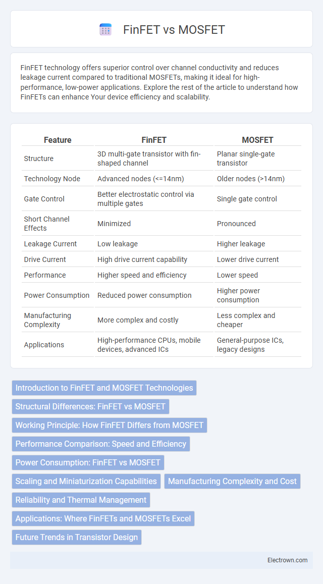
Table of Comparison
| Feature | FinFET | MOSFET |
|---|---|---|
| Structure | 3D multi-gate transistor with fin-shaped channel | Planar single-gate transistor |
| Technology Node | Advanced nodes (<=14nm) | Older nodes (>14nm) |
| Gate Control | Better electrostatic control via multiple gates | Single gate control |
| Short Channel Effects | Minimized | Pronounced |
| Leakage Current | Low leakage | Higher leakage |
| Drive Current | High drive current capability | Lower drive current |
| Performance | Higher speed and efficiency | Lower speed |
| Power Consumption | Reduced power consumption | Higher power consumption |
| Manufacturing Complexity | More complex and costly | Less complex and cheaper |
| Applications | High-performance CPUs, mobile devices, advanced ICs | General-purpose ICs, legacy designs |
Introduction to FinFET and MOSFET Technologies
FinFET technology, a type of multi-gate MOSFET, enhances transistor performance by utilizing a 3D fin-shaped channel that wraps around the gate, significantly reducing short-channel effects and leakage currents compared to traditional planar MOSFETs. MOSFET (Metal-Oxide-Semiconductor Field-Effect Transistor) technology, foundational to semiconductor devices, relies on a planar structure with a flat channel beneath the gate oxide, which faces scaling challenges at sub-22nm nodes. The transition from planar MOSFETs to FinFETs enables continued device scaling, improved power efficiency, and higher switching speeds in advanced integrated circuits.
Structural Differences: FinFET vs MOSFET
FinFETs feature a three-dimensional fin-shaped channel that rises above the substrate, providing better electrostatic control and reducing short-channel effects compared to the planar channel of traditional MOSFETs. MOSFETs rely on a flat, two-dimensional channel structure with a single gate on top, limiting scalability and increasing leakage current as device dimensions shrink. The FinFET's multi-gate design enables improved performance, higher drive current, and lower power consumption, making it superior for advanced semiconductor nodes.
Working Principle: How FinFET Differs from MOSFET
FinFET differs from traditional MOSFET by using a three-dimensional fin-shaped channel that wraps around the gate, enabling better electrostatic control over the channel and significantly reducing short-channel effects. MOSFET operates with a planar channel where the gate controls the transistor by creating an electric field perpendicular to the channel surface. The FinFET's multi-gate structure enhances current flow efficiency, reduces leakage current, and improves scalability for advanced semiconductor technologies compared to the single-gate MOSFET design.
Performance Comparison: Speed and Efficiency
FinFET technology offers significantly higher speed and improved power efficiency compared to traditional MOSFETs due to its 3D structure, which reduces leakage current and enhances gate control. This results in faster switching speeds and lower power consumption, making FinFETs ideal for advanced processors and high-performance computing devices. Your choice of FinFET over MOSFET can lead to better overall performance in speed-critical and energy-sensitive applications.
Power Consumption: FinFET vs MOSFET
FinFET technology significantly reduces power consumption compared to traditional MOSFETs by minimizing leakage currents and enhancing control over the channel with its 3D gate structure. This advanced design leads to lower static power dissipation and improved energy efficiency, making FinFETs ideal for low-power, high-performance applications. Your devices can achieve better battery life and thermal management when utilizing FinFET-based transistors instead of conventional MOSFETs.
Scaling and Miniaturization Capabilities
FinFETs exhibit superior scaling and miniaturization capabilities compared to traditional planar MOSFETs, enabling smaller gate lengths and higher density integration on semiconductor chips. The 3D structure of FinFETs significantly reduces short-channel effects and leakage currents, allowing device dimensions to shrink below the 10 nm node while maintaining performance and power efficiency. This advancement supports continued adherence to Moore's Law by enabling ultra-scaled transistors with enhanced electrostatic control and lower variability.
Manufacturing Complexity and Cost
FinFET devices require advanced 3D nanofabrication techniques, increasing manufacturing complexity compared to traditional planar MOSFETs, which rely on well-established, simpler processes. The intricate fin structures in FinFETs demand precise lithography and etching, leading to higher production costs and longer development times. Your choice between FinFET and MOSFET technology must consider these manufacturing challenges alongside performance benefits in semiconductor device design.
Reliability and Thermal Management
FinFET devices exhibit superior reliability compared to traditional MOSFETs due to their three-dimensional multi-gate structure, which reduces short-channel effects and leakage currents, enhancing device stability under high electric fields. Thermal management in FinFETs benefits from a smaller footprint and improved heat dissipation pathways, allowing better handling of self-heating issues prevalent in advanced semiconductor nodes. MOSFETs typically face greater challenges with hot carrier degradation and negative bias temperature instability, while FinFETs achieve extended lifespan and performance consistency through improved electrothermal characteristics.
Applications: Where FinFETs and MOSFETs Excel
FinFETs excel in high-performance computing and advanced mobile devices where reduced leakage current and enhanced switching speeds are critical, making them ideal for cutting-edge processors and low-power applications. MOSFETs remain dominant in power electronics, analog circuits, and cost-sensitive applications due to their simpler fabrication and proven reliability. Your choice between FinFET and MOSFET technology depends on the specific performance requirements and power efficiency goals of your electronic design.
Future Trends in Transistor Design
FinFET technology offers superior control over short-channel effects and reduced leakage currents compared to traditional MOSFETs, making it a preferred choice for advanced semiconductor nodes below 10nm. Emerging transistor designs, such as Gate-All-Around (GAA) FETs and nanosheet transistors, build upon FinFET architecture to enhance performance and scaling efficiency further. Your semiconductor devices will benefit from these innovations, achieving higher speed, lower power consumption, and improved thermal management in future integrated circuits.
FinFET vs MOSFET Infographic