Planar transistors feature a flat channel, making them simpler to manufacture but less efficient at controlling current leakage compared to FinFETs, which utilize a 3D fin-shaped channel to enhance performance and power efficiency. Discover how these differences impact your device's speed, power consumption, and scalability by reading the full article.
Table of Comparison
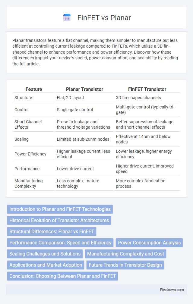
| Feature | Planar Transistor | FinFET Transistor |
|---|---|---|
| Structure | Flat, 2D layout | 3D fin-shaped channels |
| Control | Single gate control | Multi-gate control (typically tri-gate) |
| Short Channel Effects | Prone to leakage and threshold voltage variations | Better suppression of leakage and short channel effects |
| Scaling | Limited at sub-20nm nodes | Effective at 14nm and below nodes |
| Power Efficiency | Higher leakage current, less efficient | Lower leakage, higher energy efficiency |
| Performance | Lower drive current | Higher drive current, improved speed |
| Manufacturing Complexity | Less complex, mature technology | More complex fabrication process |
Introduction to Planar and FinFET Technologies
Planar and FinFET technologies represent two distinct approaches in semiconductor device architecture, with Planar transistors using a flat channel structure while FinFETs feature a 3D fin-like channel that enhances control over current flow. FinFET technology offers improved performance and power efficiency by reducing leakage currents and enabling higher transistor density compared to Planar devices. Your choice between these technologies impacts the scalability and energy efficiency of modern integrated circuits, particularly at advanced process nodes below 20 nanometers.
Historical Evolution of Transistor Architectures
The historical evolution of transistor architectures highlights the transition from planar transistors, which dominated semiconductor manufacturing from the 1960s to the early 2000s, to FinFETs introduced in the 2010s to combat short-channel effects and improve performance at smaller nodes. Planar transistors rely on a flat channel and gate structure, whereas FinFETs utilize a 3D fin-shaped channel that enhances gate control and reduces leakage currents, enabling lower power consumption and higher speed at advanced technology nodes like 7nm and below. Your choice of semiconductor technology depends on factors such as integration density, power efficiency, and device scaling limitations addressed by FinFET architecture compared to traditional planar designs.
Structural Differences: Planar vs FinFET
Planar transistors feature a flat, horizontal channel structure where current flows parallel to the substrate, whereas FinFETs utilize a vertical fin-shaped channel that protrudes from the substrate, enabling better control of the channel by wrapping the gate around three sides. This 3D architecture in FinFETs reduces short-channel effects and leakage current, leading to improved performance and energy efficiency at smaller technology nodes. Your device's scaling benefits significantly from FinFET's structural innovation compared to the traditional planar design.
Performance Comparison: Speed and Efficiency
FinFET technology offers significantly higher speed and energy efficiency compared to traditional planar transistors by reducing short-channel effects and improving current control. The three-dimensional structure of FinFETs enhances carrier mobility, enabling faster switching speeds and lower power consumption, which is critical for high-performance computing. Your devices benefit from FinFET's superior transistor density, delivering improved overall performance and battery life in modern processors.
Power Consumption Analysis
Planar transistors exhibit higher leakage current and reduced control over short-channel effects, leading to increased power consumption compared to FinFETs. FinFET technology significantly lowers static power by enhancing gate control with a 3D structure, minimizing subthreshold leakage and improving energy efficiency. As a result, FinFETs are preferred in modern low-power applications, offering superior performance-per-watt for advanced semiconductor nodes below 20nm.
Scaling Challenges and Solutions
Planar transistors face significant scaling challenges due to increased short-channel effects and leakage currents as device dimensions shrink below 20 nm. FinFET technology addresses these issues with a 3D structure that provides better electrostatic control over the channel, reducing leakage and improving performance at advanced nodes like 7 nm and 5 nm. Solutions such as multi-gate designs and advanced doping techniques further enhance FinFET scalability, enabling continued transistor density improvements under Moore's Law.
Manufacturing Complexity and Cost
Planar transistors feature simpler, more mature manufacturing processes that generally result in lower production costs compared to FinFETs. FinFET technology involves complex 3D structuring and advanced lithography, increasing fabrication difficulty and expenses. The added process steps and precision required for FinFET yield higher initial investment and operational costs despite delivering superior performance.
Applications and Market Adoption
Planar transistors remain prevalent in low-power and cost-sensitive applications such as microcontrollers and analog circuits due to their simpler manufacturing process and lower production costs. FinFET technology dominates high-performance computing markets, including CPUs and GPUs, because of superior energy efficiency and enhanced switching speed at smaller nodes. Your choice between Planar and FinFET depends on application requirements, balancing cost and performance demands within current semiconductor market trends.
Future Trends in Transistor Design
Planar transistors have dominated semiconductor design but are increasingly challenged by scaling limitations and leakage currents as nodes shrink below 10nm. FinFET technology addresses these issues with 3D gate structures, improving electrostatic control and power efficiency, positioning it as the current industry standard. Future trends point toward Gate-All-Around (GAA) transistors and nanosheet architectures overcoming FinFET barriers, enabling further miniaturization and enhanced performance to meet Your needs for high-speed, low-power devices.
Conclusion: Choosing Between Planar and FinFET
Choosing between Planar and FinFET technology depends on the specific application requirements, including power efficiency, performance, and manufacturing complexity. FinFETs offer superior control over short-channel effects and reduced leakage current, making them ideal for advanced nodes below 22nm. Planar transistors remain cost-effective for mature nodes and less demanding performance targets, providing a balance between manufacturing yield and device reliability.
Planar vs FinFET Infographic