Thick oxide layers offer increased durability and better insulation, while thin oxides provide superior speed and performance in semiconductor devices. Explore the article to understand how the choice between thick oxide and thin oxide impacts Your device's efficiency and reliability.
Table of Comparison
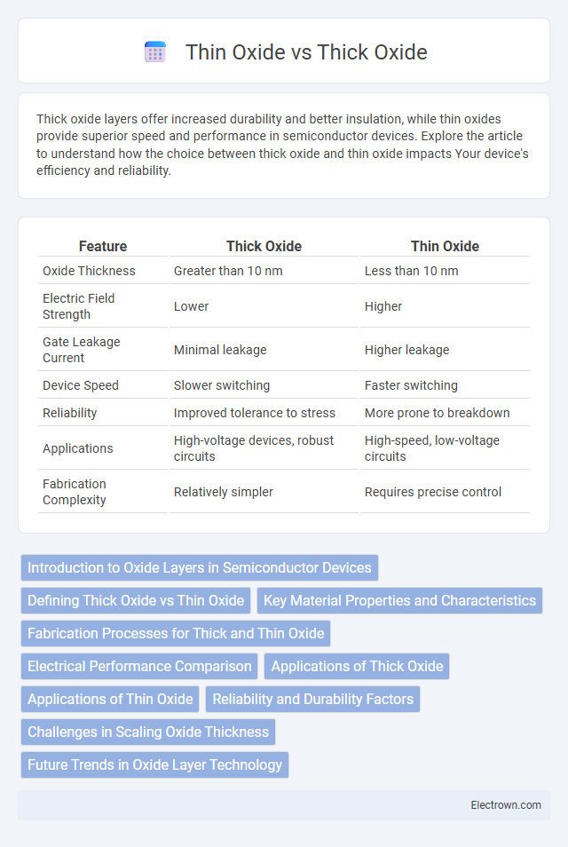
| Feature | Thick Oxide | Thin Oxide |
|---|---|---|
| Oxide Thickness | Greater than 10 nm | Less than 10 nm |
| Electric Field Strength | Lower | Higher |
| Gate Leakage Current | Minimal leakage | Higher leakage |
| Device Speed | Slower switching | Faster switching |
| Reliability | Improved tolerance to stress | More prone to breakdown |
| Applications | High-voltage devices, robust circuits | High-speed, low-voltage circuits |
| Fabrication Complexity | Relatively simpler | Requires precise control |
Introduction to Oxide Layers in Semiconductor Devices
Oxide layers in semiconductor devices serve as crucial insulating barriers that influence device performance, with thick oxide offering robust insulation and thin oxide enabling precise control of electrical properties at the nanoscale. Thin oxide layers, typically ranging from a few nanometers to tens of nanometers, are essential in transistor gate oxides for enhanced switching speeds and reduced power consumption. Understanding the differences between thick and thin oxide layers enables you to optimize device design for reliability and efficiency in advanced semiconductor applications.
Defining Thick Oxide vs Thin Oxide
Thick oxide and thin oxide refer to the layers of silicon dioxide used as insulating materials in semiconductor devices, where thick oxide layers typically exceed 100 nanometers while thin oxide layers are usually below 10 nanometers. Thick oxide provides robust insulation and is commonly used for field isolation and device protection, whereas thin oxide is essential for gate oxides in MOSFETs, ensuring precise channel control and higher device performance. Understanding the distinction between these oxide thicknesses is crucial for optimizing your semiconductor fabrication processes and enhancing device reliability.
Key Material Properties and Characteristics
Thick oxide layers exhibit greater electrical insulation and higher breakdown voltage, making them ideal for power devices and high-voltage applications. Thin oxide films provide better electron tunneling efficiency and higher capacitance, crucial for MOSFET gate dielectrics and high-speed semiconductor devices. Understanding these material properties helps optimize Your device performance and reliability based on oxide thickness requirements.
Fabrication Processes for Thick and Thin Oxide
Thick oxide fabrication typically involves thermal oxidation at higher temperatures and longer durations to grow a robust SiO2 layer used for field isolation or passivation in semiconductor devices. Thin oxide layers require precise control during rapid thermal oxidation or chemical vapor deposition to achieve ultrathin, uniform films critical for gate dielectrics in MOSFETs. Process parameters such as temperature, oxidizing ambient, and time are finely tuned to optimize electrical properties and minimize defects based on oxide thickness requirements.
Electrical Performance Comparison
Thick oxide layers exhibit higher breakdown voltages and better insulation but suffer from slower transistor switching speeds due to increased gate capacitance. Thin oxide enables faster electron tunneling and enhanced carrier mobility, resulting in superior transistor performance and lower power consumption. However, thin oxide is more prone to leakage currents and reliability issues under high electric fields, impacting long-term device stability.
Applications of Thick Oxide
Thick oxide layers are commonly used in high-voltage applications such as power transistors, insulated-gate bipolar transistors (IGBTs), and field-effect transistors (FETs) to provide enhanced electrical insulation and improve device reliability. These layers offer superior resistance to leakage currents and dielectric breakdown, making them ideal for devices operating under harsh electrical conditions. Your circuits benefit from thick oxide's robustness, especially in power management and automotive electronics where durability and safety are critical.
Applications of Thin Oxide
Thin oxide layers are essential in semiconductor device manufacturing, particularly for applications requiring high-speed switching and precise gate control in MOSFETs. They enhance device performance by reducing threshold voltage and allowing for greater transistor scaling in integrated circuits. Your electronics benefit from thin oxide's ability to improve device reliability, minimize power consumption, and increase overall processing speed in advanced microchips.
Reliability and Durability Factors
Thick oxide layers provide enhanced reliability and durability in semiconductor devices by offering better resistance to electrical breakdown and improved insulation properties under high voltage stress. Thin oxide layers, while beneficial for faster switching speeds and lower power consumption, are more susceptible to degradation mechanisms such as time-dependent dielectric breakdown (TDDB) and increased leakage currents. Your choice between thick and thin oxide should balance performance demands with long-term device stability, particularly in applications requiring robust reliability under harsh operating conditions.
Challenges in Scaling Oxide Thickness
Scaling oxide thickness in semiconductor devices presents significant challenges, including increased leakage currents and compromised gate control as oxide layers become thinner. Thick oxide layers improve reliability and reduce leakage but hinder device performance and scaling due to higher capacitance and slower switching speeds. To optimize your device performance, balancing the oxide thickness is essential to maintain electrical integrity while pushing for smaller, faster transistors.
Future Trends in Oxide Layer Technology
Future trends in oxide layer technology emphasize the development of ultra-thin oxide films for enhanced transistor performance, enabling higher speed and lower power consumption in semiconductor devices. Advanced deposition techniques such as atomic layer deposition (ALD) are being optimized to achieve atomic-scale thickness control, improving reliability and scalability in integrated circuits. Research also focuses on high-k dielectric materials to replace traditional silicon dioxide layers, reducing leakage currents and supporting miniaturization in next-generation electronics.
Thick Oxide vs Thin Oxide Infographic