Flip-chip technology offers superior electrical performance and higher density packaging compared to traditional wire-bond methods, enabling faster signal transmission and reduced parasitic inductance. Explore the key differences and advantages of each technique to understand which one best suits your electronic device needs.
Table of Comparison
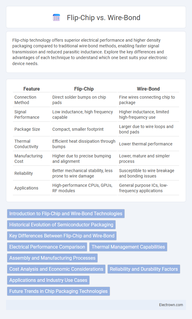
| Feature | Flip-Chip | Wire-Bond |
|---|---|---|
| Connection Method | Direct solder bumps on chip pads | Fine wires connecting chip to package |
| Signal Performance | Low inductance, high frequency capable | Higher inductance, limited high-frequency use |
| Package Size | Compact, smaller footprint | Larger due to wire loops and bond pads |
| Thermal Conductivity | Efficient heat dissipation through bumps | Lower thermal performance |
| Manufacturing Cost | Higher due to precise bumping and alignment | Lower, mature and simpler process |
| Reliability | Better mechanical stability, less prone to wire damage | Susceptible to wire breakage and bonding issues |
| Applications | High-performance CPUs, GPUs, RF modules | General purpose ICs, low-frequency applications |
Introduction to Flip-Chip and Wire-Bond Technologies
Flip-chip technology involves directly attaching semiconductor dies to substrates using solder bumps, enabling shorter interconnects and improved electrical performance. Wire-bond technology connects the die to the package via fine wires, typically gold or aluminum, offering a cost-effective and widely used solution for chip packaging. Both methods play critical roles in microelectronics, with flip-chip favored for high-frequency and high-density applications, while wire-bond remains prevalent in standard integrated circuits.
Historical Evolution of Semiconductor Packaging
The historical evolution of semiconductor packaging saw wire-bonding emerge as the dominant method in the early days, enabling reliable connections from the chip to the package leads using fine metal wires. Flip-chip technology, introduced later, revolutionized packaging by allowing direct electrical connection between the chip and substrate through solder bumps, offering improved performance, smaller form factors, and better thermal management. Your choice between flip-chip and wire-bond packaging depends on factors such as device complexity, cost constraints, and thermal requirements driven by advancements in semiconductor fabrication.
Key Differences Between Flip-Chip and Wire-Bond
Flip-chip technology offers a shorter electrical path by directly connecting the die to the substrate with solder bumps, resulting in improved performance and higher interconnect density compared to wire-bonding. Wire-bonding uses thin metal wires to link the die to the package, which is simpler and more cost-effective but has longer signal paths and lower frequency capabilities. Your choice depends on factors such as desired device size, electrical performance, manufacturing complexity, and cost constraints.
Electrical Performance Comparison
Flip-chip technology offers superior electrical performance compared to wire-bonding due to shorter interconnect lengths and lower inductance, resulting in reduced signal delay and enhanced high-frequency response. The decreased parasitic capacitance and resistance in flip-chip assemblies enable higher current densities and improved power integrity. In contrast, wire-bond connections introduce larger parasitic elements, leading to increased signal distortion and limited bandwidth performance.
Thermal Management Capabilities
Flip-chip technology offers superior thermal management capabilities compared to wire-bonding by enabling a direct connection between the semiconductor die and the substrate, which enhances heat dissipation through shorter thermal paths. Wire-bonding relies on thin metal wires that create longer thermal resistance paths, potentially leading to higher junction temperatures. Optimizing your device's thermal performance is often more effective with flip-chip due to its improved heat spread and reduced thermal impedance.
Assembly and Manufacturing Processes
Flip-chip assembly involves directly mounting the semiconductor die onto the substrate with solder bumps, enabling shorter interconnects and higher electrical performance compared to wire-bond techniques. Wire-bond manufacturing uses fine gold or aluminum wires to connect the die pads to the package leads, which is simpler but can introduce longer signal paths and higher inductance. Selecting between flip-chip and wire-bond processes impacts your device's signal integrity, assembly complexity, and overall manufacturing cost.
Cost Analysis and Economic Considerations
Flip-chip technology generally incurs higher initial manufacturing costs compared to wire-bond due to expensive bumping processes and sophisticated equipment requirements. Wire-bonding offers lower upfront investment and better compatibility with established assembly lines, making it more cost-effective for low to medium volume production. Economically, flip-chip provides advantages in performance and miniaturization, which can reduce system-level costs in high-volume or high-performance applications despite the higher per-unit manufacturing expense.
Reliability and Durability Factors
Flip-chip technology offers superior reliability and durability due to its short electrical paths and robust solder bump connections, reducing signal inductance and enhancing thermal performance compared to traditional wire-bond methods. Wire-bonding faces challenges such as wire lift, bond pad damage, and susceptibility to mechanical stress, which can compromise long-term device integrity. Your choice between flip-chip and wire-bond should consider these reliability factors, especially for applications requiring high thermal cycling endurance and mechanical robustness.
Applications and Industry Use Cases
Flip-chip technology is widely adopted in high-performance computing, mobile devices, and automotive electronics due to its superior electrical performance and heat dissipation capabilities. Wire-bonding remains prevalent in cost-sensitive applications such as consumer electronics, power devices, and LED packaging, where its manufacturing simplicity and reliability are advantageous. Industries like telecommunications and aerospace often prefer flip-chip for advanced system integration, while wire-bond continues to dominate in sensor modules and general-purpose semiconductor packaging.
Future Trends in Chip Packaging Technologies
Flip-chip technology is advancing with trends such as fine-pitch interconnects, 3D stacking, and heterogeneous integration, enabling higher performance and reduced latency in semiconductor devices. Wire-bonding remains relevant due to its cost-effectiveness and flexibility but is gradually supplemented by flip-chip solutions in high-density, high-frequency applications. Emerging packaging technologies like fan-out wafer-level packaging (FOWLP) and chiplet architectures are shaping the future, combining the benefits of both flip-chip and wire-bond methods to meet demands for miniaturization and enhanced thermal management.
Flip-Chip vs Wire-Bond Infographic