Self-aligned gate technology improves transistor performance by precisely aligning the gate with the source and drain regions, reducing parasitic capacitance and enhancing switching speed, unlike non-self-aligned gate designs which often suffer from alignment inaccuracies and increased leakage currents. Explore this article to understand how these differences impact your semiconductor device's efficiency and scalability.
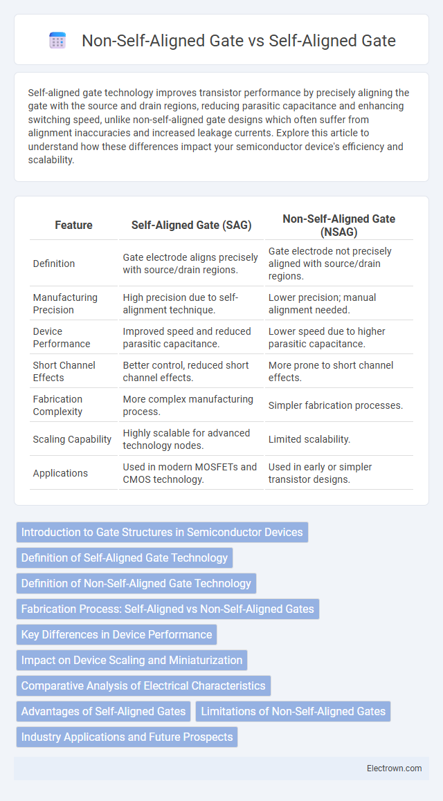
Table of Comparison
| Feature | Self-Aligned Gate (SAG) | Non-Self-Aligned Gate (NSAG) |
|---|---|---|
| Definition | Gate electrode aligns precisely with source/drain regions. | Gate electrode not precisely aligned with source/drain regions. |
| Manufacturing Precision | High precision due to self-alignment technique. | Lower precision; manual alignment needed. |
| Device Performance | Improved speed and reduced parasitic capacitance. | Lower speed due to higher parasitic capacitance. |
| Short Channel Effects | Better control, reduced short channel effects. | More prone to short channel effects. |
| Fabrication Complexity | More complex manufacturing process. | Simpler fabrication processes. |
| Scaling Capability | Highly scalable for advanced technology nodes. | Limited scalability. |
| Applications | Used in modern MOSFETs and CMOS technology. | Used in early or simpler transistor designs. |
Introduction to Gate Structures in Semiconductor Devices
Self-aligned gate structures in semiconductor devices enable precise alignment between the gate electrode and source/drain regions, significantly reducing parasitic capacitance and enhancing transistor performance. Non-self-aligned gates, created through separate lithography steps, often suffer from misalignment issues that increase overlap capacitance and limit device scaling. The self-aligned process ensures minimal gate-to-source/drain overlap, improving drive current and enabling higher integration density in advanced CMOS technologies.
Definition of Self-Aligned Gate Technology
Self-Aligned Gate technology refers to a fabrication process in semiconductor manufacturing where the gate electrode of a MOSFET is precisely aligned with the source and drain regions, minimizing the overlap and parasitic capacitances. This alignment enhances device performance by reducing short-channel effects and improving current drive capability. Your semiconductor devices benefit from increased speed and power efficiency due to the reduced gate-to-source/drain misalignment inherent in Self-Aligned Gate designs compared to Non-Self-Aligned Gates.
Definition of Non-Self-Aligned Gate Technology
Non-self-aligned gate technology refers to a transistor fabrication method where the gate electrode is not precisely aligned with the source and drain regions, leading to overlap or gaps that affect device performance. This misalignment often results in increased parasitic capacitance and reduced switching speed compared to self-aligned gate devices. Non-self-aligned gates are typically used in older or simpler semiconductor processes, where precise gate alignment techniques are not implemented.
Fabrication Process: Self-Aligned vs Non-Self-Aligned Gates
Self-aligned gate fabrication utilizes the gate electrode itself as a mask to define the source and drain regions, enabling precise alignment that minimizes parasitic capacitance and enhances device performance. Non-self-aligned gate processes rely on separate lithography steps for source/drain implantation, which can lead to misalignment, increased overlap capacitance, and reduced transistor speed. The self-aligned approach is critical in advanced CMOS technologies to achieve higher integration density and improved electrical characteristics.
Key Differences in Device Performance
Self-aligned gate transistors exhibit significantly reduced parasitic capacitance and improved short-channel control compared to non-self-aligned gate devices, leading to enhanced switching speeds and lower power consumption. The precise alignment in self-aligned gates minimizes overlap between the gate and source/drain regions, reducing leakage currents and boosting device reliability. Non-self-aligned gates often suffer from increased series resistance and variability in threshold voltage, which adversely affect overall device performance and scalability in advanced semiconductor technologies.
Impact on Device Scaling and Miniaturization
Self-aligned gate technology significantly improves device scaling and miniaturization by reducing parasitic capacitance and enhancing channel control, enabling smaller, faster, and more power-efficient transistors. Non-self-aligned gate structures face limitations due to misalignment between gate and source/drain regions, causing increased short-channel effects and degraded device performance as dimensions shrink. Your ability to achieve ultra-scaled semiconductor devices is greatly enhanced using self-aligned gate processes, which are crucial for advancing modern nanoelectronics.
Comparative Analysis of Electrical Characteristics
Self-aligned gate technology significantly reduces parasitic capacitances by precisely aligning the gate electrode with the source and drain regions, enhancing device speed and frequency response compared to non-self-aligned gate devices. Non-self-aligned gates exhibit higher overlap capacitance leading to increased leakage currents and degraded subthreshold slope, impacting overall power efficiency. Your choice between these technologies affects device performance metrics such as transconductance, threshold voltage stability, and switching speed, making self-aligned gates preferable for high-performance integrated circuits.
Advantages of Self-Aligned Gates
Self-aligned gates significantly reduce parasitic capacitance and resistance by precisely aligning the gate electrode with the source and drain regions, leading to enhanced transistor switching speed and overall device performance. This alignment improves channel control, minimizing short-channel effects and leakage currents in advanced CMOS technologies. Consequently, self-aligned gates enable higher integration density and power efficiency in modern semiconductor devices compared to non-self-aligned gate structures.
Limitations of Non-Self-Aligned Gates
Non-Self-Aligned Gates suffer from increased parasitic capacitance and resistance due to misalignment between the gate and the source/drain regions, leading to degraded device performance. This misalignment causes higher short-channel effects and reduced drive current, limiting transistor scalability and speed. Your designs benefit from self-aligned gates by minimizing overlap and enhancing electrical characteristics, which are difficult to achieve with non-self-aligned structures.
Industry Applications and Future Prospects
Self-aligned gate technology enhances transistor performance by reducing parasitic capacitance, making it ideal for high-speed integrated circuits in the semiconductor industry. Non-self-aligned gates, while simpler and cheaper, are typically used in lower-performance applications such as analog circuits and memory devices. Your choice between these gate types impacts the scalability and efficiency of future electronic devices, with self-aligned gates driving advancements in nanoscale technology and energy-efficient chips.
Self-Aligned Gate vs Non-Self-Aligned Gate Infographic