Double poly processes enhance durability and insulation by adding an extra polyethylene layer, improving your product's performance and longevity. Discover how choosing between double poly and single poly processes can impact the quality and cost-effectiveness of your project by reading the full article.
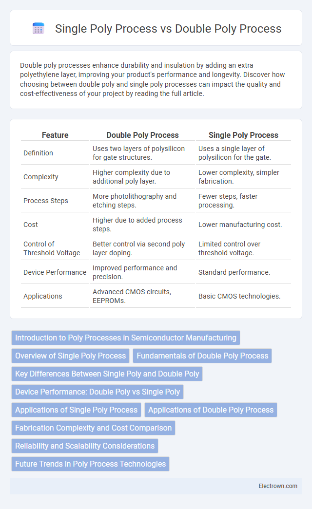
Table of Comparison
| Feature | Double Poly Process | Single Poly Process |
|---|---|---|
| Definition | Uses two layers of polysilicon for gate structures. | Uses a single layer of polysilicon for the gate. |
| Complexity | Higher complexity due to additional poly layer. | Lower complexity, simpler fabrication. |
| Process Steps | More photolithography and etching steps. | Fewer steps, faster processing. |
| Cost | Higher due to added process steps. | Lower manufacturing cost. |
| Control of Threshold Voltage | Better control via second poly layer doping. | Limited control over threshold voltage. |
| Device Performance | Improved performance and precision. | Standard performance. |
| Applications | Advanced CMOS circuits, EEPROMs. | Basic CMOS technologies. |
Introduction to Poly Processes in Semiconductor Manufacturing
Double poly and single poly processes are foundational techniques in semiconductor manufacturing used to create multiple layers of polysilicon for transistor gates and interconnects. The double poly process allows for enhanced device complexity and improved performance by enabling layered gate structures and capacitors, while the single poly process is simpler and suited for less complex circuits. Both methods utilize polysilicon as a gate material, critical for controlling electrical properties in MOSFET devices.
Overview of Single Poly Process
The Single Poly Process involves fabricating transistors using a single layer of polysilicon, which simplifies manufacturing and reduces cost compared to double poly techniques. It enables efficient gate formation but may limit design flexibility and device performance in advanced integrated circuits. Understanding this process helps you evaluate semiconductor options based on application requirements and fabrication complexity.
Fundamentals of Double Poly Process
The Double Poly Process involves two layers of polysilicon: a thin gate poly depleted of carriers and a thick poly for interconnects, enhancing transistor performance by reducing threshold voltage variability and improving electrical stability. This approach separates gate doping from the interconnect layer, allowing precise control over gate characteristics while maintaining robust metal-like connectivity. By optimizing gate oxide integrity and minimizing polysilicon depletion effects, the Double Poly Process enables higher-speed, lower-leakage CMOS devices ideal for advanced semiconductor technologies.
Key Differences Between Single Poly and Double Poly
The key differences between single poly and double poly processes lie in their manufacturing techniques and material layering; single poly involves a single layer of polymer, offering lighter weight and simpler production, while double poly incorporates two polymer layers, enhancing durability and chemical resistance. Double poly is typically preferred for applications requiring higher mechanical strength and better barrier properties, whereas single poly is suitable for less demanding environments due to its cost-effectiveness. Your choice depends on the required balance between performance and budget constraints in specific industrial or packaging applications.
Device Performance: Double Poly vs Single Poly
Double Poly technology enhances device performance by enabling the formation of more complex gate structures, which improves threshold voltage control and reduces short-channel effects compared to Single Poly processes. The additional polysilicon layer in Double Poly devices allows for better gate capacitance tuning, resulting in faster switching speeds and lower leakage currents. In contrast, Single Poly devices offer simpler fabrication but may experience higher variability and limited scaling potential, impacting overall device reliability and efficiency.
Applications of Single Poly Process
The Single Poly Process is primarily utilized in the fabrication of simple digital logic devices and memory components where cost-effectiveness and reduced complexity are critical. It is often applied in the manufacture of basic CMOS logic circuits, EEPROMs, and certain types of analog components where a single polysilicon layer suffices for gate formation. This process enables streamlined silicon chip designs, offering lower production costs while maintaining adequate performance for less complex semiconductor applications.
Applications of Double Poly Process
Double Poly process is widely used in CMOS technology for fabricating non-volatile memory devices, such as EEPROMs and Flash memory, due to its ability to create floating gates for charge storage. You will find this process advantageous in applications requiring reliable charge trapping and enhanced data retention over standard Single Poly methods. The precise control of gate dimensions and electrical isolation in Double Poly enables improved device performance in embedded memory and analog integrated circuits.
Fabrication Complexity and Cost Comparison
Double poly process involves two sequential polysilicon layer depositions separated by an interlayer dielectric, resulting in increased fabrication complexity compared to the single poly process, which uses only one polysilicon layer. This complexity in double poly fabrication leads to higher production costs due to additional photolithography steps and process controls. Your choice between the two processes should consider the trade-off between enhanced device functionality in double poly and the lower cost and simplicity of single poly fabrication.
Reliability and Scalability Considerations
The double poly process offers enhanced reliability by incorporating a second polysilicon layer that improves gate control and reduces short-channel effects, leading to more stable transistor performance under varying operational conditions. Scalability is also superior in double poly technology, as it enables finer device geometries and better threshold voltage tuning, making it suitable for advanced semiconductor nodes compared to the single poly process. Single poly processes, while simpler and cost-effective, tend to face challenges with leakage currents and variability at smaller scales, limiting their use in high-performance and highly scalable applications.
Future Trends in Poly Process Technologies
Future trends in poly process technologies are shifting towards advanced double poly processes due to their enhanced scalability and improved dielectric properties, which are critical for next-generation semiconductor devices. Innovations in double poly techniques emphasize reducing parasitic capacitance and enabling higher-density integration, essential for 3D NAND and advanced logic applications. Single poly processes, while simpler and cost-effective, are gradually being supplemented by double poly methods to meet the demand for increased performance and miniaturization in emerging tech nodes.
Double Poly vs Single Poly Process Infographic