Schottky diodes offer faster switching speeds and lower forward voltage drops compared to PN junction diodes, making them ideal for high-frequency and low-voltage applications. Discover how these differences impact your electronic designs by reading the rest of the article.
Table of Comparison
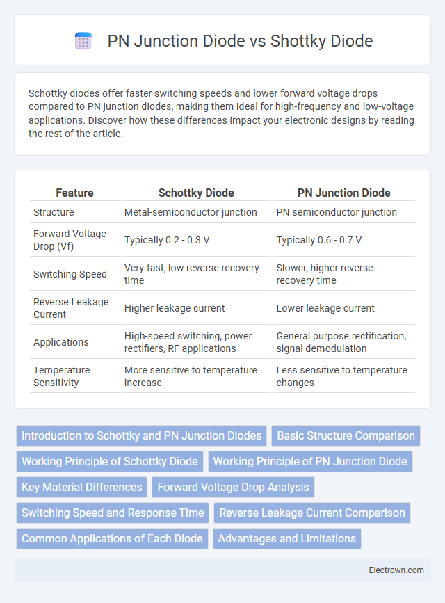
| Feature | Schottky Diode | PN Junction Diode |
|---|---|---|
| Structure | Metal-semiconductor junction | PN semiconductor junction |
| Forward Voltage Drop (Vf) | Typically 0.2 - 0.3 V | Typically 0.6 - 0.7 V |
| Switching Speed | Very fast, low reverse recovery time | Slower, higher reverse recovery time |
| Reverse Leakage Current | Higher leakage current | Lower leakage current |
| Applications | High-speed switching, power rectifiers, RF applications | General purpose rectification, signal demodulation |
| Temperature Sensitivity | More sensitive to temperature increase | Less sensitive to temperature changes |
Introduction to Schottky and PN Junction Diodes
Schottky diodes utilize a metal-semiconductor junction, resulting in faster switching speeds and lower forward voltage drops compared to PN junction diodes, which are formed by p-type and n-type semiconductor materials creating a depletion region. The unique metal-semiconductor interface in Schottky diodes minimizes charge storage, enhancing efficiency in high-frequency applications, whereas PN junction diodes exhibit higher reverse recovery time due to minority carrier recombination. These intrinsic differences influence their performance in power rectification, signal detection, and switching circuits within electronic devices.
Basic Structure Comparison
The Schottky diode features a metal-semiconductor junction, typically made by contacting a metal with an n-type semiconductor, resulting in a low forward voltage drop and fast switching speed. The PN junction diode consists of a p-type semiconductor joined with an n-type semiconductor, creating a depletion region that controls current flow with higher forward voltage and slower response. Understanding the basic structural differences helps you select the appropriate diode for applications requiring high efficiency or fast switching.
Working Principle of Schottky Diode
The Schottky diode operates based on the metal-semiconductor junction where electrons move from the semiconductor to the metal, creating a low forward voltage drop and faster switching speed. Unlike the PN junction diode that relies on the depletion region formed between p-type and n-type semiconductors, the Schottky diode avoids minority carrier charge storage, resulting in minimal reverse recovery time. This unique working principle makes Schottky diodes ideal for high-frequency and low-voltage power applications.
Working Principle of PN Junction Diode
The working principle of a PN junction diode relies on the formation of a depletion region at the junction of p-type and n-type semiconductors, where charge carriers recombine and create a barrier that allows current to flow primarily in one direction. When forward biased, this barrier is reduced, enabling significant current flow as electrons and holes cross the junction. Understanding this mechanism is essential for comparing the PN junction diode's performance with the faster switching and lower forward voltage drop characteristics of a Schottky diode.
Key Material Differences
Schottky diodes use a metal-semiconductor junction, typically involving materials like platinum, gold, or tungsten on n-type silicon, which results in lower forward voltage drop and faster switching speed. PN junction diodes are made from p-type and n-type semiconductor materials, primarily silicon or germanium, forming a depletion region that controls current flow. Your choice depends on whether you prioritize speed and efficiency (Schottky diode) or higher voltage tolerance and lower leakage current (PN junction diode).
Forward Voltage Drop Analysis
Schottky diodes exhibit a lower forward voltage drop, typically around 0.2 to 0.3 volts, compared to the 0.6 to 0.7 volts found in PN junction diodes, resulting in higher efficiency and reduced heat dissipation in power-sensitive applications. This characteristic enables faster switching speeds and lower power loss, making Schottky diodes ideal for high-frequency circuits and rectification tasks. The metal-semiconductor junction in Schottky diodes minimizes charge carrier recombination, directly influencing the reduced forward voltage and improved performance in energy-sensitive environments.
Switching Speed and Response Time
Schottky diodes offer significantly faster switching speeds and lower response times compared to PN junction diodes due to their metal-semiconductor junction, which lacks the charge storage effects found in PN junctions. This characteristic makes Schottky diodes ideal for high-frequency applications and efficient power rectification. Your choice of diode will impact the performance of circuits requiring rapid switching and minimal delay.
Reverse Leakage Current Comparison
Schottky diodes exhibit significantly lower reverse leakage current compared to PN junction diodes due to their metal-semiconductor junction, which results in a lower built-in potential barrier. Typical Schottky diodes have reverse leakage currents in the microampere range at room temperature, whereas PN junction diodes can exhibit leakage currents in the nanoampere to microampere range depending on doping and temperature. This characteristic makes Schottky diodes especially suitable for high-speed switching and low-power applications where leakage current minimization is critical.
Common Applications of Each Diode
Shottky diodes are commonly used in high-speed switching applications, power rectification, and voltage clamping due to their low forward voltage drop and fast recovery time. PN junction diodes find widespread use in general rectification, signal demodulation, and voltage regulation where higher forward voltage and slower switching speeds are acceptable. Your choice between these diodes depends on the required efficiency and speed for circuits like power supplies or radio frequency detectors.
Advantages and Limitations
Schottky diodes offer faster switching speeds and lower forward voltage drop (typically 0.2-0.3V) compared to PN junction diodes, making them ideal for high-frequency and low-voltage applications. However, Schottky diodes have lower reverse voltage ratings and higher leakage currents, which can limit their use in high-voltage circuits. Understanding these advantages and limitations helps you select the right diode based on efficiency, speed, and voltage requirements.
Shottky Diode vs PN Junction Diode Infographic