JTAG and SWD are two debugging protocols used for microcontroller programming and testing, with JTAG offering more pin connections and compatibility across a wider range of devices, while SWD provides a simpler two-pin interface optimized for ARM Cortex processors. Explore the rest of the article to understand which interface best suits your development needs and how to implement them effectively.
Table of Comparison
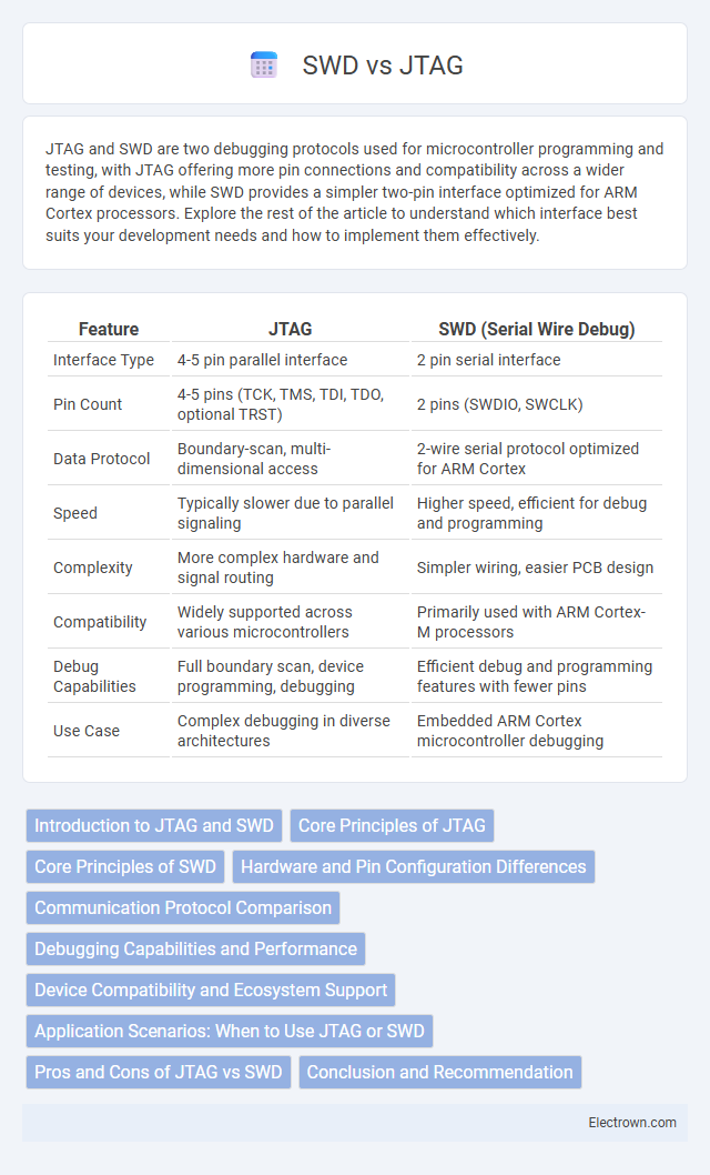
| Feature | JTAG | SWD (Serial Wire Debug) |
|---|---|---|
| Interface Type | 4-5 pin parallel interface | 2 pin serial interface |
| Pin Count | 4-5 pins (TCK, TMS, TDI, TDO, optional TRST) | 2 pins (SWDIO, SWCLK) |
| Data Protocol | Boundary-scan, multi-dimensional access | 2-wire serial protocol optimized for ARM Cortex |
| Speed | Typically slower due to parallel signaling | Higher speed, efficient for debug and programming |
| Complexity | More complex hardware and signal routing | Simpler wiring, easier PCB design |
| Compatibility | Widely supported across various microcontrollers | Primarily used with ARM Cortex-M processors |
| Debug Capabilities | Full boundary scan, device programming, debugging | Efficient debug and programming features with fewer pins |
| Use Case | Complex debugging in diverse architectures | Embedded ARM Cortex microcontroller debugging |
Introduction to JTAG and SWD
JTAG (Joint Test Action Group) and SWD (Serial Wire Debug) are protocols used for debugging and programming embedded systems. JTAG operates using a multi-pin interface widely supported across various microcontrollers and processors, enabling boundary-scan testing and device programming. SWD, developed by ARM, provides a more efficient two-pin interface specifically designed for ARM Cortex devices, offering fast and streamlined debugging with reduced pin count.
Core Principles of JTAG
JTAG (Joint Test Action Group) core principles revolve around boundary-scan architecture, enabling testing and debugging of integrated circuits through a standardized 4 or 5-pin interface. It uses a serial communication protocol with Test Access Port (TAP) controllers to shift data into and out of device registers, facilitating device programming, fault detection, and real-time debugging. The JTAG standard (IEEE 1149.1) supports complex multi-device chain configurations, enhancing test coverage and system diagnostics in embedded systems.
Core Principles of SWD
SWD (Serial Wire Debug) uses a two-wire interface consisting of a clock (SWCLK) and a data line (SWDIO) to communicate with ARM Cortex-M microcontrollers, offering a simpler and more pin-efficient alternative to JTAG's multi-line approach. Unlike JTAG, which requires multiple pins and supports a broader range of devices, SWD focuses on minimal pin usage and efficient debugging performance specifically for ARM cores. Your development process benefits from SWD's streamlined protocol, which enables fast and reliable access to the CPU's debug and control registers.
Hardware and Pin Configuration Differences
JTAG (Joint Test Action Group) interfaces typically use a 5 to 20-pin connector including TCK, TMS, TDI, TDO, and GND, enabling multi-device testing and boundary scan operations. SWD (Serial Wire Debug) is a streamlined alternative using only two pins--SWDIO and SWCLK--along with GND, simplifying hardware requirements and reducing board space. Your choice between JTAG and SWD will impact the complexity of your hardware design and connector layout due to these pin configuration differences.
Communication Protocol Comparison
JTAG (Joint Test Action Group) uses a 4- to 5-wire interface supporting boundary-scan architecture for comprehensive device testing and debugging, making it ideal for complex multi-chip systems. SWD (Serial Wire Debug) employs a 2-wire interface optimized for low-pin-count microcontrollers, providing a simpler, faster communication protocol with reduced hardware overhead. Your choice depends on the required signal complexity, speed, and hardware resources of your embedded development environment.
Debugging Capabilities and Performance
JTAG and SWD both offer powerful debugging capabilities, with JTAG supporting multi-core processors and extensive boundary-scan testing, while SWD is optimized for single-core ARM Cortex devices, providing faster data transfer speeds and lower pin count. JTAG's parallel interface allows for broad device compatibility and complex system diagnostics, but its multiple-pin requirement can limit performance in compact designs. SWD's serial interface enhances debugging efficiency through quicker halt and run commands, making it ideal for modern embedded applications prioritizing performance and minimal hardware footprint.
Device Compatibility and Ecosystem Support
JTAG supports a wider range of devices across various manufacturers, making it compatible with many legacy and modern microcontrollers and processors, while SWD is primarily designed for ARM Cortex-M series, offering streamlined debugging in that ecosystem. The JTAG ecosystem includes extensive tools and debuggers from multiple vendors, providing broad interoperability, whereas SWD benefits from integrated support in ARM development environments and specialized tooling optimized for low-pin-count applications. Device compatibility with JTAG is often favored in complex, multi-core systems, whereas SWD excels in compact, resource-constrained ARM microcontroller debugging scenarios.
Application Scenarios: When to Use JTAG or SWD
JTAG is ideal for complex embedded systems requiring boundary scan testing and multi-device debugging support, commonly used in FPGAs and multi-core processors. SWD (Serial Wire Debug) is suited for low-pin count ARM Cortex-M microcontrollers where efficient, reduced-pin connectivity is essential. Your choice depends on device architecture and debugging needs--use JTAG for comprehensive testing and SWD for simpler, resource-constrained applications.
Pros and Cons of JTAG vs SWD
JTAG offers extensive debugging capabilities with support for multiple devices in a chain, making it ideal for complex system designs, but it requires more pins and can be slower compared to SWD. SWD, designed for ARM Cortex processors, provides a simpler two-pin interface that reduces board complexity and increases debugging speed, though it supports fewer devices and less extensive features than JTAG. Your choice depends on system complexity and pin availability, balancing comprehensive debugging (JTAG) against streamlined efficiency (SWD).
Conclusion and Recommendation
JTAG offers a versatile debugging interface supporting multiple cores and extensive boundary-scan testing, making it suitable for complex system designs and multi-chip environments. SWD provides a streamlined, low-pin alternative optimized for ARM Cortex-M processors, enabling efficient debugging with reduced hardware overhead. For resource-constrained embedded projects prioritizing simplicity and faster debug cycles, SWD is recommended, whereas JTAG remains the preferred choice for advanced system-level diagnostics and multi-core debugging.
JTAG vs SWD Infographic