Bandgap modulation alters the energy difference between the valence and conduction bands in a material, directly impacting its electrical and optical properties. Understanding the differences between bandgap modulation and workfunction modulation can help you optimize device performance; explore the rest of the article to learn more.
Table of Comparison
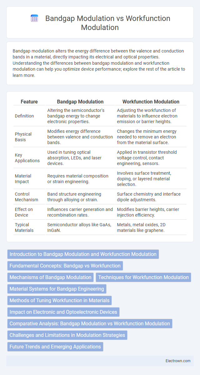
| Feature | Bandgap Modulation | Workfunction Modulation |
|---|---|---|
| Definition | Altering the semiconductor's bandgap energy to change electronic properties. | Adjusting the workfunction of materials to influence electron emission or barrier heights. |
| Physical Basis | Modifies energy difference between valence and conduction bands. | Changes the minimum energy needed to remove an electron from the material surface. |
| Key Applications | Used in tuning optical absorption, LEDs, and laser devices. | Applied in transistor threshold voltage control, contact engineering, sensors. |
| Material Impact | Requires material composition or strain engineering. | Involves surface treatment, doping, or layered material selection. |
| Control Mechanism | Band structure engineering through alloying or strain. | Surface chemistry and interface dipole adjustments. |
| Effect on Device | Influences carrier generation and recombination rates. | Modifies barrier heights, carrier injection efficiency. |
| Typical Materials | Semiconductor alloys like GaAs, InGaN. | Metals, metal oxides, 2D materials like graphene. |
Introduction to Bandgap Modulation and Workfunction Modulation
Bandgap modulation involves tuning the energy difference between the valence and conduction bands in semiconductors, directly affecting their electrical and optical properties. Workfunction modulation refers to altering the minimum energy required to remove an electron from a material's surface, influencing charge injection and extraction in electronic devices. Both techniques are essential for optimizing device performance in applications like transistors, sensors, and photovoltaics.
Fundamental Concepts: Bandgap vs Workfunction
Bandgap modulation involves altering the energy difference between the valence band and conduction band in a semiconductor, directly impacting its electrical conductivity and optical properties. Workfunction modulation changes the minimum energy required to remove an electron from the material's surface, influencing electron emission and contact properties in electronic devices. Understanding these fundamental concepts helps you tailor semiconductor behavior for optimized device performance.
Mechanisms of Bandgap Modulation
Bandgap modulation primarily occurs through mechanisms like quantum confinement, strain engineering, and alloy composition variation, which alter the energy difference between the valence and conduction bands in semiconductors. This adjustment affects electronic and optical properties by directly tuning the bandgap energy, enabling customizable device performance. Your ability to manipulate these factors allows precise control over semiconductor behavior in applications such as transistors, lasers, and photodetectors.
Techniques for Workfunction Modulation
Techniques for workfunction modulation primarily include surface engineering methods such as atomic layer deposition, self-assembled monolayers, and plasma treatments to tailor the electronic properties of materials. Utilizing metal alloying and doping strategies also effectively adjusts the workfunction by altering the intrinsic electronic structure. These approaches enable precise control of charge injection barriers critical for optimizing device performance in applications like organic electronics and semiconductor interfaces.
Material Systems for Bandgap Engineering
Material systems for bandgap engineering primarily include III-V semiconductors like GaAs and InP, as well as II-VI compounds such as ZnSe, enabling precise control over electronic and optical properties through compositional tuning. Alloying and heterostructures in these materials allow for bandgap modulation critical for applications in optoelectronics and photovoltaics. Your selection of materials directly influences device performance by tailoring bandgap energy rather than relying solely on workfunction modulation, which affects surface electronic states.
Methods of Tuning Workfunction in Materials
Workfunction modulation in materials is primarily achieved through surface engineering, such as chemical doping, adsorption of molecular layers, and interface dipole formation, which alter the electron affinity and surface potential. Atomic layer deposition and plasma treatments enable precise control of surface termination and defect states, thereby adjusting the workfunction with high accuracy. Metal-organic frameworks and two-dimensional materials provide tunable platforms by varying their composition and structural defects, offering versatile methods for optimizing electronic and optoelectronic device performance.
Impact on Electronic and Optoelectronic Devices
Bandgap modulation directly alters a material's electronic band structure, enabling precise control over carrier concentration and recombination rates, which enhances the efficiency of optoelectronic devices like LEDs and solar cells. Workfunction modulation influences the energy barrier at interfaces, affecting charge injection and extraction in electronic devices such as transistors and photodetectors, thereby optimizing device performance and reducing power consumption. Your choice between these modulations depends on the targeted application, as bandgap engineering primarily tunes intrinsic electronic properties, while workfunction adjustment critically manages interface phenomena.
Comparative Analysis: Bandgap Modulation vs Workfunction Modulation
Bandgap modulation directly alters the intrinsic energy gap in semiconductor materials, influencing carrier concentration and device switching characteristics, while workfunction modulation primarily affects the surface potential and carrier injection thresholds by adjusting the metal-semiconductor interface properties. Bandgap engineering offers tunable electronic and optical properties suitable for high-performance transistors and optoelectronic devices, whereas workfunction modulation enables precise control over contact resistance and threshold voltage in field-effect transistors. When optimizing Your device performance, selecting bandgap modulation is preferable for intrinsic material property tuning, whereas workfunction modulation is advantageous for interface and contact-level adjustments.
Challenges and Limitations in Modulation Strategies
Bandgap modulation faces challenges such as material stability and precise control over bandgap width, limiting its effectiveness in dynamic electronic applications. Workfunction modulation encounters difficulties in achieving uniform surface modification and maintaining long-term stability under operational conditions. Your choice between these strategies depends on balancing device performance requirements with fabrication complexity and environmental robustness.
Future Trends and Emerging Applications
Bandgap modulation offers precise control over electronic and optoelectronic properties, making it essential for next-generation flexible electronics and high-efficiency solar cells. Workfunction modulation plays a critical role in tailoring contact interfaces for low-power transistors and sensors, enabling advancements in wearable technology and neuromorphic computing. Your ability to leverage these modulation techniques will drive innovation in energy harvesting devices and adaptive electronic systems.
Bandgap modulation vs Workfunction modulation Infographic