Strain engineering and doping are two advanced techniques used to enhance semiconductor performance by modifying material properties; strain engineering alters the crystal lattice to improve carrier mobility, while doping introduces specific impurities to control electrical conductivity. Discover how these methods differ and which one suits Your semiconductor applications by reading the full article.
Table of Comparison
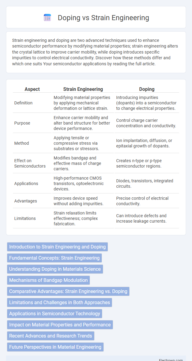
| Aspect | Strain Engineering | Doping |
|---|---|---|
| Definition | Modifying material properties by applying mechanical deformation or lattice strain. | Introducing impurities (dopants) into a semiconductor to change electrical properties. |
| Purpose | Enhance carrier mobility and alter band structure for better device performance. | Control charge carrier concentration and conductivity. |
| Method | Applying tensile or compressive stress via substrates or stressors. | Ion implantation, diffusion, or epitaxial growth of dopants. |
| Effect on Semiconductors | Modifies bandgap and effective mass of charge carriers. | Creates n-type or p-type semiconductor regions. |
| Applications | High-performance CMOS transistors, optoelectronic devices. | Diodes, transistors, integrated circuits. |
| Advantages | Improves device speed without adding impurities. | Precise control of electrical conductivity. |
| Limitations | Strain relaxation limits effectiveness; complex fabrication. | Can introduce defects and increase leakage currents. |
Introduction to Strain Engineering and Doping
Strain engineering involves the deliberate deformation of semiconductor crystal lattices to enhance electronic properties such as carrier mobility and bandgap tuning. Doping introduces impurity atoms into a semiconductor to control its electrical conductivity by increasing free charge carriers. Both techniques are essential in semiconductor device fabrication, with strain engineering primarily optimizing performance and doping enabling precise electrical control.
Fundamental Concepts: Strain Engineering
Strain engineering involves intentionally deforming a material's crystal lattice to modify its electronic, optical, or mechanical properties without introducing impurities. This technique enhances carrier mobility and alters band structure by applying tensile or compressive strain, crucial for optimizing semiconductor device performance. Your ability to control strain at the nanoscale offers precise tuning of material characteristics beyond conventional doping methods.
Understanding Doping in Materials Science
Doping in materials science involves intentionally introducing impurities into a semiconductor to modulate its electrical properties, enhancing conductivity by increasing charge carriers. This process is critical for creating p-type or n-type materials, essential for the functionality of electronic devices like transistors and diodes. Understanding how doping alters band structures and carrier concentrations helps you optimize material performance in advanced technological applications.
Mechanisms of Bandgap Modulation
Strain engineering modulates the bandgap by altering the lattice constants of materials, inducing changes in atomic spacing that directly affect electronic band structures and enhance carrier mobility. Doping modifies the bandgap through the introduction of impurity atoms, creating localized energy states within the band structure that influence electrical conductivity and carrier concentration. Your choice between strain engineering and doping depends on the desired modulation precision and the specific application requirements of semiconductor devices.
Comparative Advantages: Strain Engineering vs. Doping
Strain engineering enhances semiconductor performance by altering lattice constants to improve carrier mobility without introducing impurity atoms, preserving crystal integrity and reducing scattering effects. Doping adjusts electrical properties by introducing specific impurity atoms to control charge carrier concentration, offering precise control over conductivity and threshold voltage. Strain engineering is advantageous for boosting speed and drive current in transistors, while doping remains essential for defining p-type and n-type regions in integrated circuits.
Limitations and Challenges in Both Approaches
Strain engineering faces limitations such as mechanical breakdown and non-uniform strain distribution, which can induce defects and negatively impact device reliability. Doping challenges include precise control over dopant concentration and diffusion, leading to variability in electrical properties and increased leakage currents. Both approaches struggle with scalability in advanced semiconductor manufacturing, where maintaining consistency at the nanoscale is critical for high-performance devices.
Applications in Semiconductor Technology
Strain engineering enhances semiconductor device performance by altering the crystal lattice to improve carrier mobility, crucial for advanced transistors and high-speed integrated circuits. Doping introduces specific impurities into semiconductors to precisely control electrical conductivity, fundamental for creating p-n junctions in diodes and transistors. Both techniques are essential in semiconductor technology, with strain engineering optimizing electron and hole transport, while doping defines the electrical characteristics needed for device functionality.
Impact on Material Properties and Performance
Strain engineering modifies the atomic lattice structure of materials, enhancing electronic mobility and mechanical flexibility by altering bandgap and carrier effective mass. Doping introduces impurity atoms into semiconductors, significantly changing electrical conductivity and carrier concentration, crucial for device functionality. Your choice between strain engineering and doping depends on whether the goal is to improve intrinsic material performance or to tailor electrical characteristics for specific applications.
Recent Advances and Research Trends
Recent advances in strain engineering emphasize precisely manipulating lattice structures to enhance electronic and optical properties of semiconductors without introducing impurities, contrasting traditional doping methods that rely on adding foreign atoms to modify conductivity. Research trends highlight the synergistic integration of strain engineering with advanced doping techniques to achieve superior performance in nano-electronic devices, including enhanced carrier mobility and reduced power consumption. Emerging studies explore strain-induced bandgap modulation combined with controlled dopant distribution for applications in next-generation transistors and quantum computing elements.
Future Perspectives in Material Engineering
Strain engineering and doping both play pivotal roles in the future of material engineering by enhancing electronic, optical, and mechanical properties at the atomic level. Strain engineering manipulates lattice structures to improve carrier mobility and device performance without the introduction of impurities, while doping adjusts electrical conductivity through controlled impurity incorporation. Your optimization of materials for next-generation semiconductors and flexible electronics will increasingly leverage these techniques to achieve unprecedented efficiency and functionality.
Strain Engineering vs Doping Infographic