Vertical nanowires offer superior density and enhanced electrical performance due to their perpendicular orientation, allowing more efficient charge transport and better integration in 3D architectures. Explore the rest of the article to understand how your choice between vertical and horizontal nanowires impacts device design and functionality.
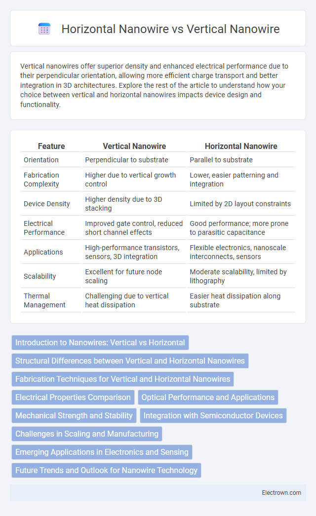
Table of Comparison
| Feature | Vertical Nanowire | Horizontal Nanowire |
|---|---|---|
| Orientation | Perpendicular to substrate | Parallel to substrate |
| Fabrication Complexity | Higher due to vertical growth control | Lower, easier patterning and integration |
| Device Density | Higher density due to 3D stacking | Limited by 2D layout constraints |
| Electrical Performance | Improved gate control, reduced short channel effects | Good performance; more prone to parasitic capacitance |
| Applications | High-performance transistors, sensors, 3D integration | Flexible electronics, nanoscale interconnects, sensors |
| Scalability | Excellent for future node scaling | Moderate scalability, limited by lithography |
| Thermal Management | Challenging due to vertical heat dissipation | Easier heat dissipation along substrate |
Introduction to Nanowires: Vertical vs Horizontal
Vertical nanowires are aligned perpendicular to the substrate, offering high packing density and enhanced electron transport for applications in sensors, transistors, and solar cells. Horizontal nanowires lie flat on the substrate, facilitating easier integration into planar circuits and enabling efficient electrical interfacing in nanoscale devices. The choice between vertical and horizontal nanowire configurations impacts fabrication complexity, device performance, and suitability for specific nanotechnology applications.
Structural Differences between Vertical and Horizontal Nanowires
Vertical nanowires are oriented perpendicular to the substrate, enabling higher device density and better electrostatic control in transistors by minimizing short-channel effects. Horizontal nanowires lie parallel to the substrate, facilitating easier integration with existing planar fabrication processes but often facing challenges in scaling and electrostatic performance. The structural orientation significantly influences electron mobility, contact resistance, and thermal management, making vertical nanowires more suitable for advanced nanoscale electronic applications.
Fabrication Techniques for Vertical and Horizontal Nanowires
Vertical nanowires are typically fabricated using bottom-up techniques such as vapor-liquid-solid (VLS) growth, molecular beam epitaxy (MBE), and chemical vapor deposition (CVD), allowing precise control over diameter, length, and composition. Horizontal nanowires are commonly produced via top-down approaches like electron beam lithography (EBL) followed by reactive ion etching (RIE), or by transferring bottom-up grown wires onto substrates for planar device integration. The choice of fabrication method directly influences structural uniformity, alignment, and scalability for applications in electronics and photonics.
Electrical Properties Comparison
Vertical nanowires exhibit superior charge carrier mobility and enhanced electron confinement compared to horizontal nanowires, leading to improved electrical conductivity and reduced scattering effects. Horizontal nanowires often face challenges with increased surface scattering and lower carrier mobility due to substrate-induced defects and alignment issues. The vertical orientation facilitates better electrostatic control and scalability in nanoscale transistors, contributing to higher on-state current and improved device performance.
Optical Performance and Applications
Vertical nanowires offer superior optical performance due to enhanced light trapping and increased surface area, making them ideal for high-efficiency photodetectors and solar cells. Horizontal nanowires provide better integration in planar device architectures, suitable for flexible electronics and nanoscale transistors. Your choice depends on whether optimizing light absorption or device integration is more critical for your specific optical application.
Mechanical Strength and Stability
Vertical nanowires exhibit superior mechanical strength and stability due to their axial load-bearing capability, which enhances resistance to bending and deformation compared to horizontal nanowires. The vertical orientation also facilitates better integration with substrates, reducing mechanical stress and improving overall device durability. Horizontal nanowires, while easier to fabricate in planar configurations, typically suffer from lower mechanical robustness due to increased susceptibility to lateral forces and surface interactions.
Integration with Semiconductor Devices
Vertical nanowires offer superior integration with semiconductor devices by enabling high-density, three-dimensional architectures that enhance device performance and scalability. Horizontal nanowires facilitate easier alignment and patterning on planar substrates, making them suitable for conventional fabrication methods in integrated circuits. The choice between vertical and horizontal nanowires impacts device efficiency, with vertical structures supporting better electrostatic control and horizontal configurations offering simpler integration for sensors and transistors.
Challenges in Scaling and Manufacturing
Scaling vertical nanowires faces challenges such as uniformity control across large wafer areas and precise alignment during lithography, complicating mass production. Horizontal nanowires encounter difficulties in maintaining consistent electrical properties due to variability in diameter and surface roughness during synthesis. Manufacturing complexities for both types include integration with existing CMOS technology and achieving reliable contacts at the nanoscale, limiting scalability and yield in commercial applications.
Emerging Applications in Electronics and Sensing
Vertical nanowires exhibit superior surface-to-volume ratios and enhanced electron mobility, making them ideal for high-sensitivity chemical and biological sensors. Horizontal nanowires offer easier integration into planar circuits, benefiting flexible electronics and nanoscale transistors. Both configurations are revolutionizing applications in nanoelectronics, with vertical arrays enabling high-density data storage and horizontal nanowires advancing wearable sensor technologies.
Future Trends and Outlook for Nanowire Technology
Vertical nanowire structures offer superior scalability and enhanced electrical performance, making them a key focus for next-generation semiconductor devices. Horizontal nanowires provide design flexibility and ease of integration with existing planar fabrication processes, supporting versatile applications in sensors and flexible electronics. Your choice between vertical and horizontal nanowire technology will shape future advancements in energy efficiency, miniaturization, and device functionality across various industries.
Vertical Nanowire vs Horizontal Nanowire Infographic