Plasmonics exploits the interaction between electromagnetic waves and free electrons on metal surfaces to achieve light confinement beyond the diffraction limit, while photonics relies on dielectric materials to guide and manipulate light at slightly larger scales. Understanding the key differences in how plasmonics and photonics operate at the nanoscale can enhance Your knowledge of advanced optical technologies--explore the rest of this article to discover more.
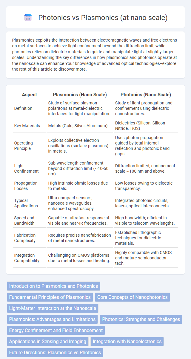
Table of Comparison
| Aspect | Plasmonics (Nano Scale) | Photonics (Nano Scale) |
|---|---|---|
| Definition | Study of surface plasmon polaritons at metal-dielectric interfaces for light manipulation. | Study of light propagation and confinement using dielectric nanostructures. |
| Key Materials | Metals (Gold, Silver, Aluminum) | Dielectrics (Silicon, Silicon Nitride, TiO2) |
| Operating Principle | Exploits collective electron oscillations (surface plasmons) in metals. | Uses photon propagation guided by total internal reflection and photonic band gaps. |
| Light Confinement | Sub-wavelength confinement beyond diffraction limit (~10-50 nm). | Diffraction limited; confinement scale ~100 nm and above. |
| Propagation Losses | High intrinsic ohmic losses due to metals. | Low losses owing to dielectric transparency. |
| Typical Applications | Ultra-compact sensors, nanoscale waveguides, enhanced spectroscopy. | Integrated photonic circuits, lasers, optical interconnects. |
| Speed and Bandwidth | Capable of ultrafast response at visible and near-IR frequencies. | High bandwidth; efficient in visible to telecom wavelengths. |
| Fabrication Complexity | Requires precise nanofabrication of metal nanostructures. | Established lithographic techniques for dielectric materials. |
| Integration Compatibility | Challenging on CMOS platforms due to metal losses and heating. | Highly compatible with CMOS and mature semiconductor tech. |
Introduction to Plasmonics and Photonics
Plasmonics explores the interaction between electromagnetic field and free electrons in metallic nanostructures, enabling confinement of light beyond the diffraction limit at the nanoscale. Photonics involves the generation, manipulation, and detection of photons using dielectric materials, typically limited by diffraction constraints. Both fields drive advances in nanoscale optics, but plasmonics offers subwavelength field enhancement while photonics excels in low-loss information transmission.
Fundamental Principles of Plasmonics
Plasmonics explores the interaction between electromagnetic fields and free electrons in metallic nanostructures, enabling light confinement beyond the diffraction limit. Surface plasmons, collective oscillations of electrons at metal-dielectric interfaces, are central to achieving enhanced optical fields at the nanoscale. Your ability to leverage these phenomena provides breakthroughs in nanoscale optical devices, surpassing traditional photonics constrained by dielectric materials.
Core Concepts of Nanophotonics
Nanophotonics explores light behavior on nanometer scales, emphasizing photon interactions with nanostructures to manipulate optical properties beyond diffraction limits. Plasmonics specifically investigates surface plasmon resonances, where conduction electrons in metallic nanostructures couple with photons, creating highly confined electromagnetic fields. Both fields enable advanced applications in sensing, imaging, and communication by exploiting light-matter interactions at the nanoscale with enhanced spatial resolution and field localization.
Light-Matter Interaction at the Nanoscale
Plasmonics exploits collective electron oscillations on metal surfaces to confine and enhance electromagnetic fields beyond the diffraction limit, enabling intense light-matter interactions at the nanoscale. Photonics, relying on dielectric materials, manipulates photons through waveguides and resonators but faces diffraction constraints that limit field confinement and enhancement. The superior field localization in plasmonics intensifies nanoscale interactions, crucial for applications like sensing, nonlinear optics, and quantum information processing.
Plasmonics: Advantages and Limitations
Plasmonics harnesses the collective oscillations of free electrons at metal-dielectric interfaces to confine light beyond the diffraction limit, enabling ultra-compact nanoscale devices with enhanced sensitivity and faster signal processing. Its advantages include subwavelength light localization and strong field enhancement, crucial for applications in biosensing, nanophotonic circuits, and quantum computing. However, plasmonics faces limitations such as significant Ohmic losses in metals, limited propagation distances, and fabrication challenges at the nanoscale, which can impact your device efficiency and integration potential compared to conventional photonics.
Photonics: Strengths and Challenges
Photonics at the nanoscale offers exceptional advantages in manipulating light with low energy loss and high-speed signal processing, enabling applications in optical communication and sensing. Its strengths include efficient light transmission through dielectric materials and compatibility with existing semiconductor technologies. Your challenge lies in overcoming the diffraction limit to achieve extreme miniaturization while maintaining performance and integration with electronic components.
Energy Confinement and Field Enhancement
Plasmonics enables exceptional energy confinement by exploiting surface plasmon resonances localized at metal-dielectric interfaces, achieving subwavelength field confinement beyond the diffraction limit, typically at tens of nanometers scale. Photonics relies on dielectric waveguides and resonators with energy confinement limited by the material refractive index contrast and diffraction to roughly half the wavelength, usually hundreds of nanometers at visible frequencies. Field enhancement in plasmonics can reach orders of magnitude higher than photonics due to strong local electromagnetic field localization around metal nanostructures, making plasmonics superior for sensing, nonlinear optics, and nanoscale light manipulation.
Applications in Sensing and Imaging
Plasmonics enables ultra-sensitive detection at the nanoscale by exploiting surface plasmon resonance, enhancing the performance of biosensors and chemical sensors beyond the diffraction limit. Photonics facilitates high-resolution imaging and real-time optical signal processing using light manipulation within nanoscale waveguides and photonic crystals. Your advancements in sensing and imaging technologies benefit from integrating plasmonic field confinement with photonic device scalability for improved sensitivity and spatial resolution.
Integration with Nanoelectronics
Plasmonics enables the manipulation of light at the nanoscale by exploiting surface plasmons, allowing seamless integration with nanoelectronic circuits due to its ability to confine electromagnetic fields beyond the diffraction limit. Photonics, while effective in guiding light through waveguides, faces challenges in miniaturization and on-chip integration at nanoscale dimensions. Your advancements in nanodevices can leverage plasmonics for higher-density, faster, and more compact optoelectronic integration compared to traditional photonic approaches.
Future Directions: Plasmonics vs Photonics
Future directions in plasmonics emphasize ultra-compact nanoscale devices exploiting surface plasmon resonances for enhanced light confinement beyond the diffraction limit, enabling breakthroughs in sensing, data storage, and quantum computing. Photonics research at the nanoscale continues to advance low-loss dielectric materials and integrated photonic circuits, prioritizing energy efficiency and high-speed optical communication. Your innovations will likely involve hybrid systems combining plasmonic field enhancement with photonic signal processing to harness the strengths of both technologies for next-generation nanoscale applications.
Plasmonics vs Photonics (at nano scale) Infographic