Top-down fabrication involves creating structures by etching away material from a larger substrate, offering precise control over pattern dimensions, while bottom-up fabrication builds structures atom-by-atom or molecule-by-molecule, enabling the assembly of complex nanostructures with unique properties. Discover how these contrasting techniques can impact your choice in advanced manufacturing by reading the full article.
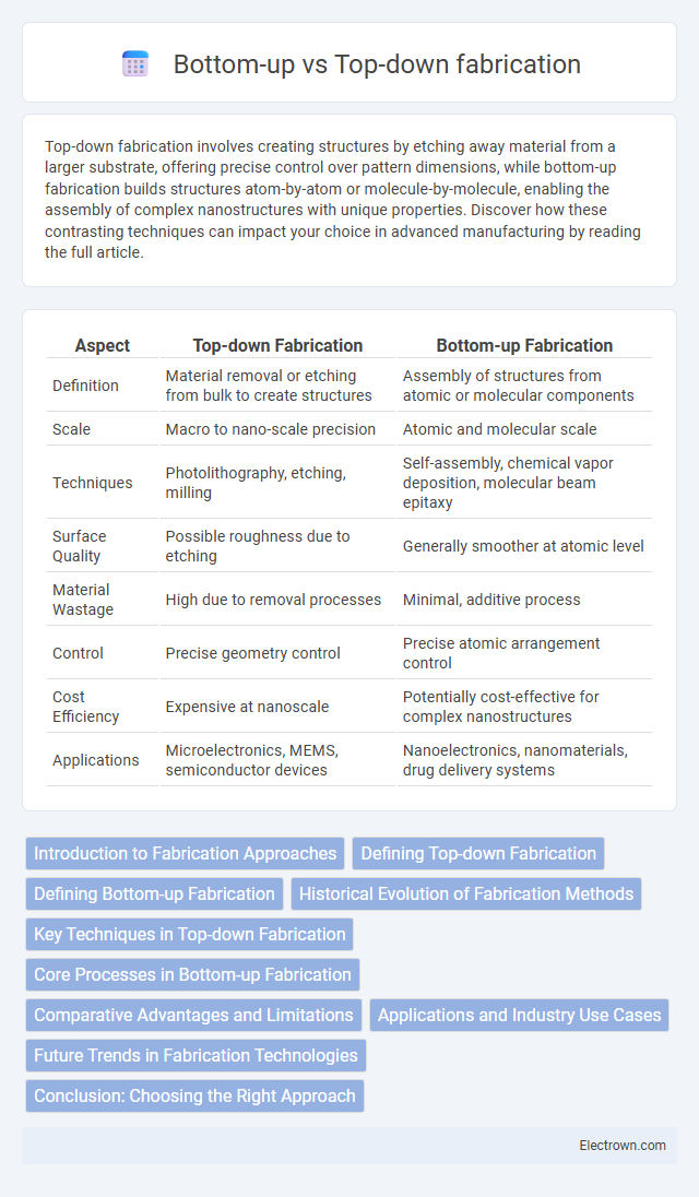
Table of Comparison
| Aspect | Top-down Fabrication | Bottom-up Fabrication |
|---|---|---|
| Definition | Material removal or etching from bulk to create structures | Assembly of structures from atomic or molecular components |
| Scale | Macro to nano-scale precision | Atomic and molecular scale |
| Techniques | Photolithography, etching, milling | Self-assembly, chemical vapor deposition, molecular beam epitaxy |
| Surface Quality | Possible roughness due to etching | Generally smoother at atomic level |
| Material Wastage | High due to removal processes | Minimal, additive process |
| Control | Precise geometry control | Precise atomic arrangement control |
| Cost Efficiency | Expensive at nanoscale | Potentially cost-effective for complex nanostructures |
| Applications | Microelectronics, MEMS, semiconductor devices | Nanoelectronics, nanomaterials, drug delivery systems |
Introduction to Fabrication Approaches
Top-down fabrication involves the controlled removal or patterning of material from bulk substrates using techniques such as photolithography and etching, enabling precise micro- and nanoscale device formation. Bottom-up fabrication assembles structures atom-by-atom or molecule-by-molecule through chemical synthesis, self-assembly, or molecular beam epitaxy, facilitating the creation of complex nanostructures. Both approaches are fundamental in semiconductor manufacturing, nanotechnology, and materials science, with top-down offering scalability and bottom-up providing atomic-level precision.
Defining Top-down Fabrication
Top-down fabrication is a manufacturing process that involves etching or removing material from a larger block to create nanoscale structures, commonly used in semiconductor and microelectronics industries. This approach relies on lithography, etching, and deposition techniques to precisely control the shape and size of features from a predetermined pattern. Understanding top-down fabrication helps you optimize device performance by ensuring high-resolution and reproducible nanoscale structures.
Defining Bottom-up Fabrication
Bottom-up fabrication constructs materials and devices atom by atom or molecule by molecule, leveraging chemical and physical processes to assemble structures from the nanoscale upward. This approach enables precise control over composition and architecture, essential for tailoring properties in nanotechnology, biotechnology, and electronics. Your ability to design complex nanostructures hinges on understanding these bottom-up synthesis techniques, including self-assembly and molecular beam epitaxy.
Historical Evolution of Fabrication Methods
Top-down fabrication methods originated during the early semiconductor era, relying on lithography and etching techniques to pattern materials from larger substrates into nanoscale devices. Bottom-up approaches emerged with advances in chemistry and molecular biology, enabling the construction of nanostructures atom-by-atom or molecule-by-molecule, offering precision beyond traditional limits. Your understanding of semiconductor manufacturing benefits from recognizing how these fabrication evolutions have shaped the transition from macro-scale processing to atomic-scale assembly in modern nanotechnology.
Key Techniques in Top-down Fabrication
Key techniques in top-down fabrication include photolithography, electron beam lithography, and reactive ion etching, which enable precise patterning and material removal from bulk substrates. Photolithography uses UV light to transfer circuit patterns onto photoresist-covered wafers, crucial for semiconductor manufacturing. Electron beam lithography offers higher resolution by directly writing patterns with a focused electron beam, supporting nanoscale device fabrication.
Core Processes in Bottom-up Fabrication
Bottom-up fabrication relies on atomic or molecular self-assembly to build structures layer by layer, essential for creating nanoscale materials with precise control over composition and properties. Core processes include chemical vapor deposition, molecular beam epitaxy, and atomic layer deposition, enabling the formation of uniform thin films and complex nanostructures. These techniques facilitate the growth of highly ordered materials used in semiconductors, catalysts, and advanced sensors, enhancing performance and miniaturization in nanotechnology applications.
Comparative Advantages and Limitations
Top-down fabrication offers precise control over feature dimensions and is well-suited for large-scale semiconductor manufacturing but involves high costs and complex processes. Bottom-up fabrication enables atomic-level precision and the creation of novel nanostructures with potentially lower material waste, yet faces challenges in scalability and uniformity. Your choice depends on whether you prioritize scalability and established technology or innovation in nanoscale design and customization.
Applications and Industry Use Cases
Top-down fabrication techniques, such as photolithography and etching, are extensively used in semiconductor manufacturing for producing integrated circuits and microelectromechanical systems (MEMS) with high precision and scalability. Bottom-up fabrication methods, including chemical vapor deposition and molecular self-assembly, are pivotal in nanotechnology applications like quantum dots, carbon nanotubes, and biosensors, enabling molecular-level control and unique material properties. Industries leveraging these approaches range from electronics and biotechnology to energy storage and advanced materials, driving innovation in microchips, flexible electronics, drug delivery systems, and next-generation batteries.
Future Trends in Fabrication Technologies
Future trends in fabrication technologies highlight increased adoption of hybrid approaches combining top-down lithography with bottom-up self-assembly to achieve unparalleled precision and scalability. Advances in nanofabrication emphasize atomic-level control through techniques such as directed self-assembly (DSA) and molecular beam epitaxy (MBE), driving breakthroughs in semiconductor manufacturing and quantum device construction. Emerging methods integrate AI-driven optimization and real-time monitoring, enhancing fabrication accuracy and enabling the production of novel materials with complex architectures at reduced costs.
Conclusion: Choosing the Right Approach
Choosing the right fabrication approach depends on your project's scale, precision, and material requirements. Top-down fabrication excels in creating complex microstructures through etching and lithography, ideal for semiconductor and MEMS production. Bottom-up fabrication offers atomic-level control and is suited for nanomaterials and molecular assembly, making it valuable for emerging nanotechnology applications.
Top-down vs Bottom-up fabrication Infographic