Hafnium oxide offers superior dielectric constant and thermal stability compared to silicon dioxide, making it a preferred gate dielectric for high-performance semiconductor devices. Explore the rest of the article to understand how this material choice impacts your device's efficiency and scaling potential.
Table of Comparison
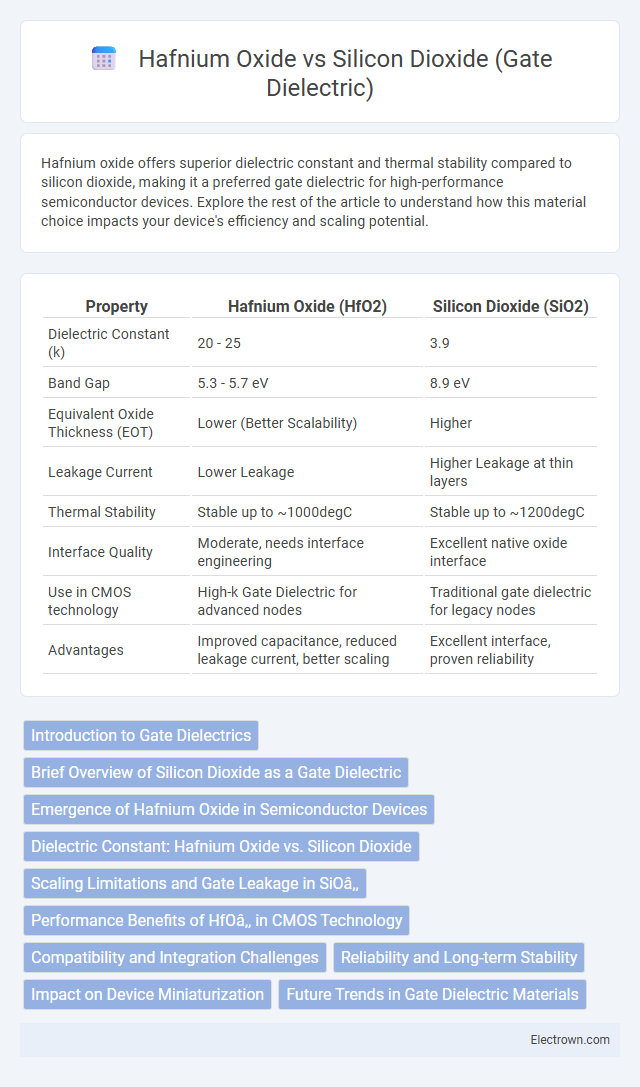
| Property | Hafnium Oxide (HfO2) | Silicon Dioxide (SiO2) |
|---|---|---|
| Dielectric Constant (k) | 20 - 25 | 3.9 |
| Band Gap | 5.3 - 5.7 eV | 8.9 eV |
| Equivalent Oxide Thickness (EOT) | Lower (Better Scalability) | Higher |
| Leakage Current | Lower Leakage | Higher Leakage at thin layers |
| Thermal Stability | Stable up to ~1000degC | Stable up to ~1200degC |
| Interface Quality | Moderate, needs interface engineering | Excellent native oxide interface |
| Use in CMOS technology | High-k Gate Dielectric for advanced nodes | Traditional gate dielectric for legacy nodes |
| Advantages | Improved capacitance, reduced leakage current, better scaling | Excellent interface, proven reliability |
Introduction to Gate Dielectrics
Gate dielectrics are critical insulating layers in transistors that control the flow of electrons without allowing current leakage. Hafnium oxide offers a high dielectric constant compared to silicon dioxide, enabling better scalability and improved performance in advanced semiconductor devices. Choosing hafnium oxide for your gate dielectric enhances drive current and reduces power consumption, making it ideal for modern microelectronics.
Brief Overview of Silicon Dioxide as a Gate Dielectric
Silicon dioxide (SiO2) has been the traditional gate dielectric material in metal-oxide-semiconductor (MOS) devices due to its excellent insulating properties, thermal stability, and ability to form a high-quality interface with silicon substrates. SiO2 possesses a dielectric constant of approximately 3.9, which limits scaling as device dimensions shrink in advanced semiconductor technology nodes. Its well-understood electrical characteristics, low leakage current, and compatibility with silicon processing have made it a benchmark gate dielectric despite challenges in achieving ultra-thin layers without increased tunneling current.
Emergence of Hafnium Oxide in Semiconductor Devices
Hafnium Oxide (HfO2) emerged as a high-k gate dielectric material to replace Silicon Dioxide (SiO2) in advanced semiconductor devices, enabling further transistor scaling beyond the 45nm node. Its high dielectric constant significantly reduces gate leakage current while maintaining excellent thermal stability and compatibility with silicon substrates. The adoption of HfO2 in CMOS technology has resulted in improved device performance, lower power consumption, and enhanced gate control in modern integrated circuits.
Dielectric Constant: Hafnium Oxide vs. Silicon Dioxide
Hafnium Oxide (HfO2) exhibits a significantly higher dielectric constant, typically around 20-25, compared to Silicon Dioxide (SiO2), which has a dielectric constant of approximately 3.9. This higher dielectric constant allows HfO2 to provide better gate capacitance and reduce leakage currents in advanced semiconductor devices. Consequently, HfO2 is preferred in modern high-k dielectric applications for improved transistor performance and scaling beyond the capabilities of SiO2.
Scaling Limitations and Gate Leakage in SiO₂
Hafnium Oxide offers superior scaling capabilities compared to Silicon Dioxide (SiO2) due to its higher dielectric constant, which allows for a physically thicker layer while maintaining equivalent capacitance, significantly reducing gate leakage currents. SiO2 faces scaling limitations as thinning beyond 1.2 nm results in unacceptable gate leakage caused by direct tunneling, impacting device reliability and power consumption. Your device performance benefits from Hafnium Oxide's ability to minimize leakage and improve electrostatic control in ultra-scaled transistors.
Performance Benefits of HfO₂ in CMOS Technology
Hafnium Oxide (HfO2) offers superior dielectric constant compared to Silicon Dioxide (SiO2), enabling greater gate capacitance without increasing gate leakage current in CMOS devices. This higher-k dielectric material improves transistor scaling by reducing power consumption and enhancing drive current, thus boosting overall performance and device reliability. You benefit from enhanced switching speeds and lower standby power, critical for modern high-performance integrated circuits.
Compatibility and Integration Challenges
Hafnium oxide (HfO2) offers superior dielectric constant compared to silicon dioxide (SiO2), enabling better gate control and scaling in advanced semiconductor devices. However, integrating HfO2 with existing silicon technology presents challenges due to interface quality issues, such as fixed charges and trap states, which can degrade device reliability and performance. Compatibility with current CMOS fabrication processes demands careful engineering of deposition techniques and post-deposition treatments to minimize defects and ensure stable electrical characteristics.
Reliability and Long-term Stability
Hafnium oxide (HfO2) exhibits superior reliability and long-term stability compared to silicon dioxide (SiO2) as a gate dielectric, due to its higher dielectric constant and enhanced resistance to breakdown and leakage currents. HfO2 enables scaling of device dimensions without significant degradation in electrical performance or increased gate leakage, maintaining stable threshold voltages over extended operational periods. In contrast, SiO2 suffers from increased electrical stress and reduced reliability at ultra-thin dimensions, limiting its effectiveness in advanced semiconductor nodes.
Impact on Device Miniaturization
Hafnium Oxide (HfO2) offers a significantly higher dielectric constant (~25) compared to Silicon Dioxide (SiO2) with a dielectric constant of about 3.9, enabling thinner gate dielectrics without leakage current issues. This high-k property of HfO2 allows further scaling of transistor gate lengths, crucial for device miniaturization in advanced semiconductor nodes. Your devices benefit from improved performance and reduced power consumption as HfO2 supports aggressive scaling beyond the physical limits of SiO2.
Future Trends in Gate Dielectric Materials
Hafnium Oxide is emerging as a superior gate dielectric material compared to Silicon Dioxide due to its higher dielectric constant, which allows for greater capacitance without scaling down thickness, effectively reducing leakage currents in advanced semiconductor devices. Future trends indicate a shift towards high-k materials like Hafnium Oxide to enable continued device scaling, improved power efficiency, and enhanced performance in next-generation transistors. Your choice of gate dielectric material will increasingly influence the balance between device miniaturization and electrical reliability in cutting-edge integrated circuits.
Hafnium Oxide vs Silicon Dioxide (gate dielectric) Infographic