Fermi level pinning significantly affects the energy barrier at metal-semiconductor interfaces by fixing the Fermi level and limiting barrier height modulation, while Schottky barrier lowering involves the reduction of this barrier under an applied electric field, enhancing charge carrier injection. Understanding these mechanisms is crucial for optimizing your device performance; explore the rest of the article to learn how they influence electronic applications.
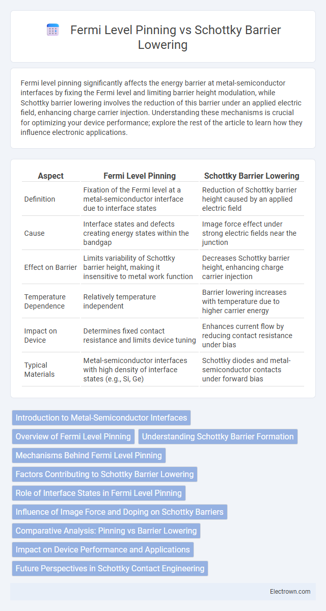
Table of Comparison
| Aspect | Fermi Level Pinning | Schottky Barrier Lowering |
|---|---|---|
| Definition | Fixation of the Fermi level at a metal-semiconductor interface due to interface states | Reduction of Schottky barrier height caused by an applied electric field |
| Cause | Interface states and defects creating energy states within the bandgap | Image force effect under strong electric fields near the junction |
| Effect on Barrier | Limits variability of Schottky barrier height, making it insensitive to metal work function | Decreases Schottky barrier height, enhancing charge carrier injection |
| Temperature Dependence | Relatively temperature independent | Barrier lowering increases with temperature due to higher carrier energy |
| Impact on Device | Determines fixed contact resistance and limits device tuning | Enhances current flow by reducing contact resistance under bias |
| Typical Materials | Metal-semiconductor interfaces with high density of interface states (e.g., Si, Ge) | Schottky diodes and metal-semiconductor contacts under forward bias |
Introduction to Metal-Semiconductor Interfaces
Metal-semiconductor interfaces are crucial in determining the electronic properties of devices, where the Fermi level pinning effect can dominate, fixing the Fermi level at the interface and limiting the ability to modulate the Schottky barrier height. Schottky barrier lowering occurs due to image force-induced barrier reduction, enabling improved charge carrier injection across the junction under applied bias conditions. Understanding these phenomena helps optimize your device performance by controlling contact resistance and energy band alignment.
Overview of Fermi Level Pinning
Fermi level pinning occurs when the energy level at the metal-semiconductor interface becomes fixed due to interface states, preventing the Schottky barrier height from varying with the metal work function. This phenomenon significantly influences charge carrier transport and limits the tunability of the Schottky barrier in electronic devices. Understanding Fermi level pinning is crucial for optimizing your device's performance by controlling interface chemistry and defect states.
Understanding Schottky Barrier Formation
Schottky barrier formation at metal-semiconductor interfaces is primarily influenced by Fermi level pinning, where interface states trap charges, fixing the Fermi level and limiting barrier height variability. This phenomenon reduces the effectiveness of Schottky barrier lowering techniques, which attempt to modulate the barrier height by external means such as doping or applied voltage. Understanding the dominant role of interface states and their density is essential for controlling contact resistance and optimizing device performance in semiconductor technology.
Mechanisms Behind Fermi Level Pinning
Fermi level pinning occurs due to the presence of metal-induced gap states (MIGS) at the metal-semiconductor interface, which trap charge and fix the Fermi level position regardless of the metal's work function. These interface states arise from the hybridization of metal wavefunctions with semiconductor states, creating a continuum of energy levels within the bandgap. This mechanism contrasts with Schottky barrier lowering, which involves image force effects that reduce the barrier height through electrostatic interactions but do not alter the intrinsic electronic states at the interface.
Factors Contributing to Schottky Barrier Lowering
Schottky barrier lowering occurs primarily due to factors such as image force-induced barrier reduction, interface states causing Fermi level pinning, and high electric fields at the metal-semiconductor junction. The presence of interface defects or impurities can modulate the local barrier height by trapping charges, thus altering electron flow in your device. Understanding these contributing elements is crucial for optimizing contact resistance and enhancing semiconductor device performance.
Role of Interface States in Fermi Level Pinning
Interface states play a crucial role in Fermi level pinning by creating energy levels within the semiconductor bandgap that trap charge carriers, effectively fixing the Fermi level at the metal-semiconductor interface. These states prevent the Schottky barrier height from being modulated by the metal work function, leading to a near-constant barrier height regardless of the metal used. The density and distribution of interface states directly influence the extent of Fermi level pinning, thereby limiting Schottky barrier lowering and affecting device performance.
Influence of Image Force and Doping on Schottky Barriers
Image force induced barrier lowering reduces the effective Schottky barrier height by creating an attractive potential that pulls charge carriers closer to the metal-semiconductor interface. Heavy doping in the semiconductor increases the electric field at the junction, enhancing image force effects and further lowering the barrier height. You can optimize device performance by carefully balancing doping concentration to mitigate Fermi level pinning while maximizing Schottky barrier reduction through image force effects.
Comparative Analysis: Pinning vs Barrier Lowering
Fermi level pinning occurs when interface states fix the Fermi level at the metal-semiconductor junction, limiting the tunability of the Schottky barrier height. Schottky barrier lowering, influenced by image force effects or applied bias, reduces the effective barrier height, enhancing carrier injection without altering the intrinsic interface states. Your device performance depends on balancing these phenomena to achieve optimal charge transport and minimize contact resistance.
Impact on Device Performance and Applications
Fermi level pinning restricts the tunability of Schottky barrier height, limiting contact resistance control and device switching speed in semiconductor-metal interfaces. Schottky barrier lowering, influenced by image force and interfacial states, enhances carrier injection efficiency, reducing turn-on voltage and improving overall device performance in diodes and transistors. Understanding these phenomena is crucial for optimizing your device's electrical characteristics and enhancing its application in high-speed electronics and optoelectronics.
Future Perspectives in Schottky Contact Engineering
Future perspectives in Schottky contact engineering focus on overcoming Fermi level pinning to achieve tunable Schottky barrier heights, enabling enhanced device performance and energy efficiency. Advanced interface passivation techniques and novel materials such as 2D semiconductors offer promising routes for reducing barrier lowering variability and increasing device stability. By controlling these parameters, your next-generation electronic and optoelectronic devices can reach improved reliability and higher operational speeds.
Fermi level pinning vs Schottky barrier lowering Infographic