Top-gate dielectric offers enhanced device stability and better interface quality, making it ideal for high-performance applications, while bottom-gate dielectric provides simpler fabrication and cost-effective solutions suitable for large-area electronics. Explore the article to understand which gate dielectric best suits your semiconductor needs.
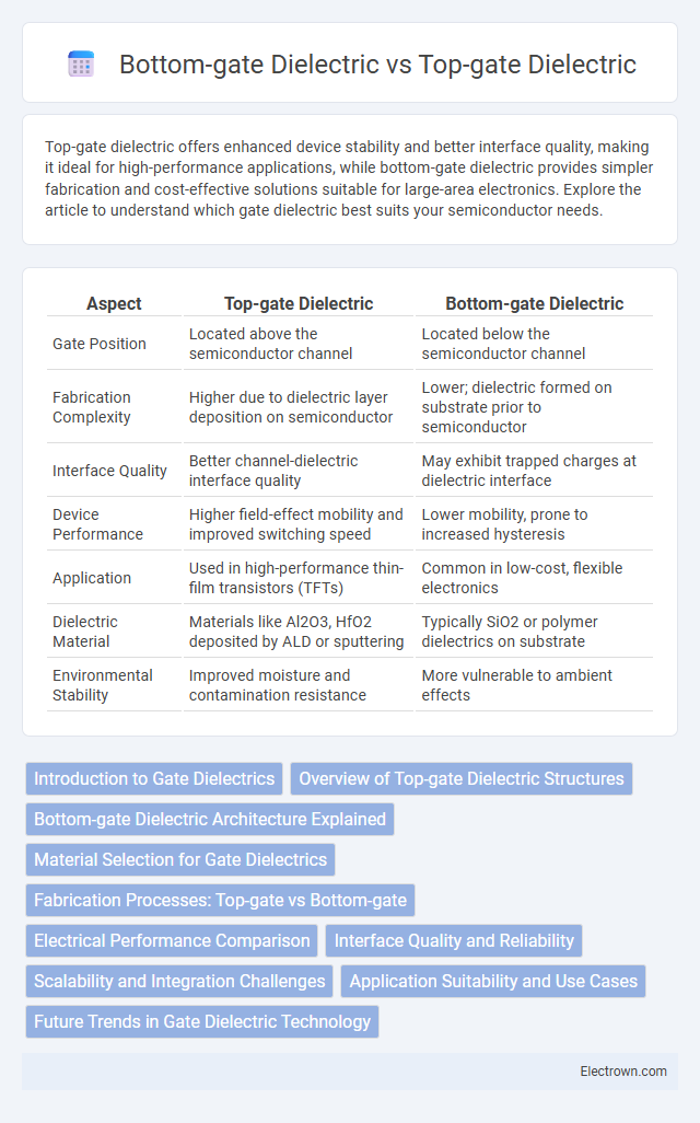
Table of Comparison
| Aspect | Top-gate Dielectric | Bottom-gate Dielectric |
|---|---|---|
| Gate Position | Located above the semiconductor channel | Located below the semiconductor channel |
| Fabrication Complexity | Higher due to dielectric layer deposition on semiconductor | Lower; dielectric formed on substrate prior to semiconductor |
| Interface Quality | Better channel-dielectric interface quality | May exhibit trapped charges at dielectric interface |
| Device Performance | Higher field-effect mobility and improved switching speed | Lower mobility, prone to increased hysteresis |
| Application | Used in high-performance thin-film transistors (TFTs) | Common in low-cost, flexible electronics |
| Dielectric Material | Materials like Al2O3, HfO2 deposited by ALD or sputtering | Typically SiO2 or polymer dielectrics on substrate |
| Environmental Stability | Improved moisture and contamination resistance | More vulnerable to ambient effects |
Introduction to Gate Dielectrics
Top-gate dielectrics are positioned above the semiconductor channel, providing enhanced control over the gate electric field and minimizing short-channel effects in advanced transistors. Bottom-gate dielectrics lie beneath the channel, offering simpler fabrication processes but potentially higher interface trap densities affecting device performance. Understanding the structural differences in your gate dielectric placement is crucial for optimizing transistor switching speed, leakage current, and overall device reliability.
Overview of Top-gate Dielectric Structures
Top-gate dielectric structures feature an insulating layer deposited above the semiconductor channel, offering enhanced control over the channel due to the proximity of the gate electrode. These structures enable better scalability and improved electrical performance by minimizing short-channel effects and reducing gate leakage current. Your choice of top-gate dielectrics can significantly impact device stability, threshold voltage, and overall transistor efficiency in advanced electronic applications.
Bottom-gate Dielectric Architecture Explained
Bottom-gate dielectric architecture places the dielectric layer beneath the semiconductor channel, enabling improved device stability and reduced short-channel effects in thin-film transistors. This configuration facilitates easier integration with common substrates like silicon wafers and supports high-k dielectrics for enhanced capacitance and leakage control. The bottom-gate design is favored in applications requiring robust gate control and scalable fabrication processes for advanced electronic circuits.
Material Selection for Gate Dielectrics
Top-gate dielectrics often utilize high-k materials such as HfO2 and Al2O3 to enhance gate capacitance and reduce leakage currents in advanced transistor architectures. Bottom-gate dielectrics frequently employ SiO2 due to its thermal stability and well-understood interface properties with silicon substrates. Choosing the appropriate gate dielectric material depends on factors like dielectric constant, interface trap density, thermal compatibility, and device scaling requirements.
Fabrication Processes: Top-gate vs Bottom-gate
Top-gate dielectric fabrication involves depositing the gate insulator and gate electrode on top of the semiconductor layer, offering better interface control and reducing surface defects. Bottom-gate dielectric processes require forming the gate dielectric and electrode beneath the semiconductor, enabling simpler back-end-of-line integration but potentially leading to higher interface trap density. Your choice between top-gate and bottom-gate dielectric fabrication impacts device performance, scalability, and compatibility with flexible substrates.
Electrical Performance Comparison
Top-gate dielectric structures exhibit superior electrical performance characterized by enhanced carrier mobility and reduced interface trap density, resulting in lower threshold voltage shifts and improved device stability. Bottom-gate dielectric devices often face challenges such as increased parasitic capacitance and higher leakage currents due to weaker gate control and poorer interface quality. Optimizing the dielectric material and thickness in top-gate configurations leads to better subthreshold swing and higher on/off current ratios compared to bottom-gate counterparts.
Interface Quality and Reliability
Top-gate dielectric structures generally exhibit superior interface quality due to better control over the dielectric-semiconductor interface, reducing charge traps and improving overall device reliability. Bottom-gate dielectrics often face challenges with interface defects and instability, which can degrade carrier mobility and increase threshold voltage shift over time. Enhanced passivation techniques in top-gate configurations contribute to improved long-term reliability and minimized hysteresis effects compared to bottom-gate counterparts.
Scalability and Integration Challenges
Top-gate dielectric structures offer superior scalability due to better electrostatic control and reduced short-channel effects, enabling aggressive device scaling in advanced semiconductor nodes. Bottom-gate dielectrics face integration challenges with higher parasitic capacitances and increased leakage currents, complicating their use in high-density circuits. The top-gate approach facilitates seamless integration with multi-gate architectures and 3D stacking, enhancing overall device performance and manufacturing yield.
Application Suitability and Use Cases
Top-gate dielectric structures offer superior control over channel formation, making them ideal for high-performance thin-film transistors used in flexible displays and sensors. Bottom-gate dielectrics provide simpler fabrication and better compatibility with large-area substrates, favoring applications like low-cost display backplanes and large-area electronics. Your choice between top-gate and bottom-gate dielectric configurations should consider specific application requirements such as scalability, electrical performance, and production costs.
Future Trends in Gate Dielectric Technology
Future trends in gate dielectric technology are shifting towards high-k materials like hafnium oxide to improve device scaling and reduce leakage currents. Top-gate dielectrics enable better electrostatic control and integration with advanced 2D materials, supporting next-generation flexible and wearable electronics. Your choice between top-gate or bottom-gate configurations will depend on the specific application requirements, including device performance and fabrication complexity.
Top-gate Dielectric vs Bottom-gate Dielectric Infographic