Heterojunction nanodevices utilize interfaces between different semiconductor materials to achieve superior electronic and optical properties, while homojunction nanodevices rely on junctions within the same material, often resulting in simpler fabrication but limited functionality. Explore the article to understand how these differences impact Your choice in advanced nanotechnology applications.
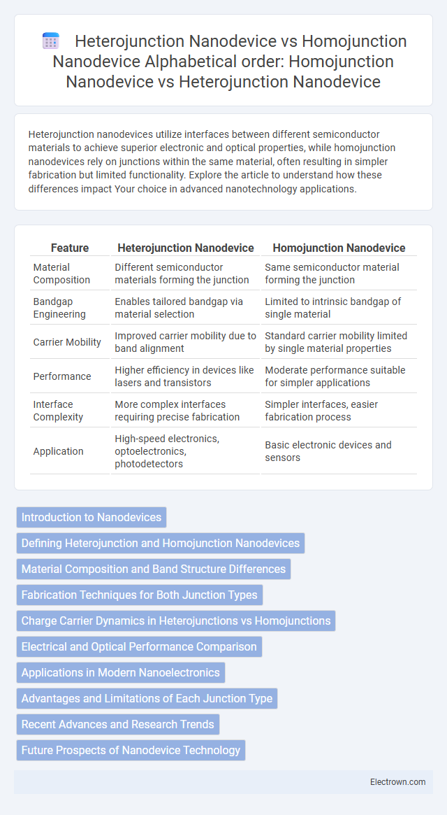
Table of Comparison
| Feature | Heterojunction Nanodevice | Homojunction Nanodevice |
|---|---|---|
| Material Composition | Different semiconductor materials forming the junction | Same semiconductor material forming the junction |
| Bandgap Engineering | Enables tailored bandgap via material selection | Limited to intrinsic bandgap of single material |
| Carrier Mobility | Improved carrier mobility due to band alignment | Standard carrier mobility limited by single material properties |
| Performance | Higher efficiency in devices like lasers and transistors | Moderate performance suitable for simpler applications |
| Interface Complexity | More complex interfaces requiring precise fabrication | Simpler interfaces, easier fabrication process |
| Application | High-speed electronics, optoelectronics, photodetectors | Basic electronic devices and sensors |
Introduction to Nanodevices
Nanodevices leverage unique properties at the nanoscale to enhance electronic and photonic performance. Heterojunction nanodevices utilize interfaces between different semiconductor materials to create superior charge carrier dynamics, while homojunction nanodevices rely on junctions within the same material, resulting in more uniform but potentially less efficient behavior. Understanding these differences helps you select the right nanodevice architecture for applications requiring optimized speed, sensitivity, or energy efficiency.
Defining Heterojunction and Homojunction Nanodevices
Heterojunction nanodevices consist of interfaces between two distinct semiconductor materials with different band gaps, enabling enhanced charge carrier separation and tailored electronic properties. Homojunction nanodevices involve junctions within the same semiconductor material, relying on doping variations to form p-n junctions with uniform crystal structure. The distinct material composition in heterojunctions offers superior performance in applications such as solar cells and transistors compared to homojunctions.
Material Composition and Band Structure Differences
Heterojunction nanodevices consist of two different semiconductor materials with distinct band gaps, creating a band discontinuity at the interface that enables enhanced charge carrier separation and transport. Homojunction nanodevices are made from a single material with uniform band structure, resulting in a continuous energy band but less efficient charge separation compared to heterojunctions. Understanding these material composition and band structure differences can help optimize your device design for specific electronic or optoelectronic applications.
Fabrication Techniques for Both Junction Types
Heterojunction nanodevices are fabricated using techniques like molecular beam epitaxy (MBE) and metal-organic chemical vapor deposition (MOCVD) to precisely deposit different semiconductor materials with controlled interfaces. Homojunction nanodevices typically rely on ion implantation and thermal diffusion to create junctions within the same semiconductor material, ensuring uniform doping profiles. Understanding these fabrication methods allows you to optimize device performance based on the distinct material interfaces in heterojunctions versus the uniformity in homojunctions.
Charge Carrier Dynamics in Heterojunctions vs Homojunctions
Charge carrier dynamics in heterojunction nanodevices differ significantly from those in homojunction nanodevices due to the presence of interface-induced band offsets that enhance carrier separation and reduce recombination rates. In heterojunctions, the discontinuity in energy bands facilitates efficient charge transfer and prolonged carrier lifetimes, improving device performance in applications like photovoltaics and photodetectors. Your device optimization can benefit from these dynamics by leveraging heterojunction structures to achieve superior charge carrier mobility and minimal recombination compared to homojunction counterparts.
Electrical and Optical Performance Comparison
Heterojunction nanodevices exhibit superior electrical performance compared to homojunction counterparts due to enhanced carrier confinement and reduced recombination rates at the interface, resulting in higher carrier mobility and improved current modulation. Optically, heterojunction nanodevices demonstrate better quantum efficiency and tunable emission wavelengths owing to bandgap engineering between different semiconductor materials, which is not achievable in homojunction nanodevices composed of the same material. Your choice between these devices depends on the need for optimized electrical conductivity and tailored optical properties in advanced nanoelectronic and optoelectronic applications.
Applications in Modern Nanoelectronics
Heterojunction nanodevices leverage the interface between two different semiconductor materials to enhance electron mobility and optimize charge separation, making them ideal for high-performance applications such as optoelectronics, photovoltaic cells, and high-speed transistors. Homojunction nanodevices, which use a single semiconductor material, are commonly employed in traditional electronic components like diodes and low-power transistors, offering simplicity and reliable performance. Your choice between these nanodevices hinges on the required device efficiency, speed, and integration complexity in modern nanoelectronic applications.
Advantages and Limitations of Each Junction Type
Heterojunction nanodevices offer superior electronic and optical properties by combining materials with different band gaps, enabling enhanced charge carrier separation and improved device efficiency in applications like solar cells and LEDs. However, lattice mismatch and interface defects can induce recombination losses, limiting performance and fabrication complexity. Homojunction nanodevices exhibit simpler fabrication due to uniform material composition, offering stable and well-understood electronic characteristics, but they often suffer from lower efficiency and limited tunability in band gap engineering compared to heterojunction systems.
Recent Advances and Research Trends
Recent advances in heterojunction nanodevices highlight superior electron mobility and energy efficiency compared to homojunction counterparts, driven by engineered interfaces between dissimilar materials enhancing charge separation. Research trends focus on integrating two-dimensional materials like graphene with transition metal dichalcogenides to optimize band alignment and improve optoelectronic performance. Your exploration of nanodevices should consider heterojunctions for cutting-edge applications in photodetectors and transistors, given their tunable electronic properties and scalability.
Future Prospects of Nanodevice Technology
Heterojunction nanodevices offer superior performance and tunability compared to homojunction nanodevices, enabling advancements in high-speed electronics and optoelectronics. Future prospects focus on leveraging the unique interface properties of heterojunctions to develop energy-efficient, multifunctional nanoscale devices. Your innovations in material engineering could drive breakthroughs in wearable technology, quantum computing, and next-generation sensors using these nanodevices.
Heterojunction Nanodevice vs Homojunction Nanodevice Infographic