Nanoconstrictions and nanogaps are critical nanoscale features used in electronic and photonic devices, where nanoconstrictions refer to narrow, continuous channels of conductive material and nanogaps are tiny insulating separations between materials. Understanding these differences can enhance your ability to optimize device performance; explore the rest of the article to learn more about their applications and fabrication techniques.
Table of Comparison
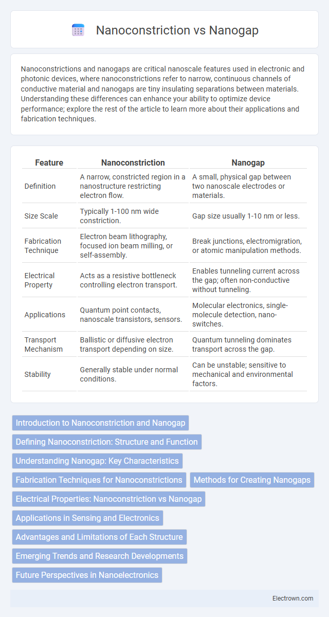
| Feature | Nanoconstriction | Nanogap |
|---|---|---|
| Definition | A narrow, constricted region in a nanostructure restricting electron flow. | A small, physical gap between two nanoscale electrodes or materials. |
| Size Scale | Typically 1-100 nm wide constriction. | Gap size usually 1-10 nm or less. |
| Fabrication Technique | Electron beam lithography, focused ion beam milling, or self-assembly. | Break junctions, electromigration, or atomic manipulation methods. |
| Electrical Property | Acts as a resistive bottleneck controlling electron transport. | Enables tunneling current across the gap; often non-conductive without tunneling. |
| Applications | Quantum point contacts, nanoscale transistors, sensors. | Molecular electronics, single-molecule detection, nano-switches. |
| Transport Mechanism | Ballistic or diffusive electron transport depending on size. | Quantum tunneling dominates transport across the gap. |
| Stability | Generally stable under normal conditions. | Can be unstable; sensitive to mechanical and environmental factors. |
Introduction to Nanoconstriction and Nanogap
Nanoconstrictions refer to extremely narrow conductive pathways typically found in nanoscale electronic devices that confine electron flow to dimensions comparable to the electron wavelength, enhancing quantum effects. Nanogaps are precisely engineered nanoscale separations between two conductive electrodes, crucial for applications like molecular electronics and single-molecule sensing. Both nanoconstrictions and nanogaps play pivotal roles in advancing nanotechnology by enabling control of electrical properties at the atomic or molecular level.
Defining Nanoconstriction: Structure and Function
Nanoconstriction refers to an ultra-narrow region within a nanostructure where the width is significantly reduced, often approaching a few nanometers, leading to quantized conductance effects and enhanced electron tunneling. This constricted geometry modulates electrical, optical, and mechanical properties, providing precise control over charge carrier flow and energy transfer at the nanoscale. Unlike nanogaps, which are discrete separations between conductive elements, nanoconstrictions maintain physical continuity while restricting carrier pathways, making them critical in quantum point contacts and nanoscale transistor applications.
Understanding Nanogap: Key Characteristics
Nanogaps are minuscule separations between conductive materials, typically measuring less than 10 nanometers, crucial in nanoscale electronic devices and sensors. These gaps facilitate quantum tunneling and electron transport mechanisms distinct from larger-scale contacts. Key characteristics include precise dimensional control, high electrical field concentration, and sensitivity to molecular interactions, making nanogaps essential for applications in molecular electronics and plasmonic devices.
Fabrication Techniques for Nanoconstrictions
Fabrication techniques for nanoconstrictions primarily involve electron beam lithography (EBL) and focused ion beam (FIB) milling, enabling precise patterning at the nanoscale. Atomic layer deposition (ALD) and electrochemical etching are also utilized to achieve controlled narrowing of conductive pathways with atomic precision. These methods produce highly reproducible nanoconstrictions crucial for nanoelectronic devices and quantum transport studies.
Methods for Creating Nanogaps
Nanogaps, essential for nanoscale electronic devices, are commonly created using electron beam lithography, focused ion beam milling, and controlled electromigration, each providing precise control at the atomic scale. Self-assembled monolayers and atomic layer deposition also enable tunable gap sizes with sub-nanometer accuracy, enhancing device performance in molecular electronics. These fabrication techniques contrast with nanoconstriction methods, which typically involve mechanical or electrochemical approaches to narrow conductive pathways without fully separating them, thus differing fundamentally in structure and application.
Electrical Properties: Nanoconstriction vs Nanogap
Nanoconstrictions exhibit significantly lower electrical resistance compared to nanogaps due to the continuous physical connection allowing electron flow, while nanogaps act as insulating barriers with electron transport primarily relying on quantum tunneling effects. The conductance in nanoconstrictions is highly sensitive to atomic-scale changes, providing precise control over electron pathways in nanoscale devices. Understanding these differences in electrical properties enables you to tailor device performance for applications in nanoelectronics and sensing technologies.
Applications in Sensing and Electronics
Nanoconstrictions and nanogaps play crucial roles in sensing and electronics by enabling ultra-sensitive detection and efficient charge transport. Nanoconstrictions, with their narrow conductive channels, allow precise control of electron flow, enhancing signal modulation in nanoelectronic devices. Nanogaps, defined by their tiny separations between electrodes, facilitate single-molecule sensing and electron tunneling, making them vital for biosensors and molecular electronics where detecting minute electrical changes is essential for Your advanced technological applications.
Advantages and Limitations of Each Structure
Nanoconstrictions offer high electrical conductance and mechanical stability, making them ideal for nanoscale sensing and switching applications, but their fabrication complexity limits scalability. Nanogaps provide exceptional sensitivity for detecting single molecules due to their ability to localize electric fields and trap particles, though they suffer from challenges in precise gap size control and long-term reliability. Both structures require advanced nanofabrication techniques, yet nanoconstrictions favor conductivity-focused devices, whereas nanogaps excel in molecular detection and quantum tunneling studies.
Emerging Trends and Research Developments
Emerging trends in nanoconstriction and nanogap research emphasize advancements in quantum transport and atomic-scale control, enabling unprecedented precision in electronic device fabrication. Recent developments highlight novel materials like graphene and transition metal dichalcogenides, significantly enhancing conductivity and tunability at the nanoscale. Your ability to leverage these innovations can drive breakthroughs in ultra-sensitive sensors and next-generation nanoelectronics.
Future Perspectives in Nanoelectronics
Nanoconstriction and nanogap technologies both hold pivotal roles in the future of nanoelectronics, with nanoconstrictions offering enhanced electron transport control and nanogaps enabling precise molecular-scale sensing. Advancements in fabrication techniques continue to push the limits of miniaturization, allowing for improved device performance and energy efficiency. Your ability to leverage these nanoscale structures will drive breakthroughs in quantum computing, ultra-sensitive sensors, and next-generation electronic circuits.
Nanoconstriction vs Nanogap Infographic