Dry etching uses plasma or gas to remove material precisely from a substrate, offering superior control and anisotropy compared to wet etching, which employs liquid chemicals and is generally less precise. Discover the detailed differences and applications to understand which etching technique best suits Your project.
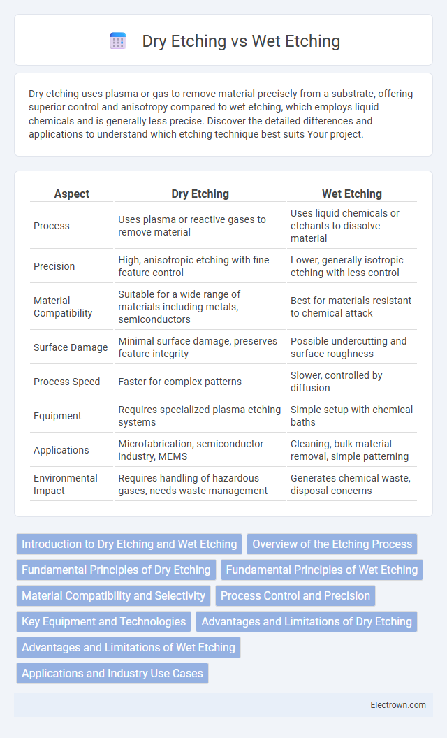
Table of Comparison
| Aspect | Dry Etching | Wet Etching |
|---|---|---|
| Process | Uses plasma or reactive gases to remove material | Uses liquid chemicals or etchants to dissolve material |
| Precision | High, anisotropic etching with fine feature control | Lower, generally isotropic etching with less control |
| Material Compatibility | Suitable for a wide range of materials including metals, semiconductors | Best for materials resistant to chemical attack |
| Surface Damage | Minimal surface damage, preserves feature integrity | Possible undercutting and surface roughness |
| Process Speed | Faster for complex patterns | Slower, controlled by diffusion |
| Equipment | Requires specialized plasma etching systems | Simple setup with chemical baths |
| Applications | Microfabrication, semiconductor industry, MEMS | Cleaning, bulk material removal, simple patterning |
| Environmental Impact | Requires handling of hazardous gases, needs waste management | Generates chemical waste, disposal concerns |
Introduction to Dry Etching and Wet Etching
Dry etching utilizes plasma or reactive gases to precisely remove material layers from semiconductor wafers, offering superior anisotropy and control for microfabrication. Wet etching employs chemical solutions to dissolve target materials, providing faster removal rates but with less directional accuracy. Both techniques are essential in semiconductor processing, with dry etching favored for fine patterning and wet etching used for bulk material removal.
Overview of the Etching Process
Dry etching utilizes plasma or ion beams to precisely remove material from a substrate, offering high anisotropy and control for semiconductor fabrication. Wet etching relies on chemical solutions to dissolve exposed areas, providing simpler equipment but limited directional control and potential undercutting. Both methods are essential in microfabrication, with dry etching preferred for intricate patterning and wet etching suited for bulk material removal.
Fundamental Principles of Dry Etching
Dry etching relies on plasma or reactive ion processes to remove material from substrates in semiconductor fabrication, enabling precise anisotropic pattern transfer. This technique utilizes chemically reactive gases ionized into plasma, which react with the surface material to form volatile byproducts that are evacuated from the chamber. Dry etching offers superior control over etch profiles and is essential for high-resolution microfabrication compared to wet etching's isotropic chemical dissolution.
Fundamental Principles of Wet Etching
Wet etching employs liquid chemical solutions to selectively remove material from a substrate through isotropic reactions that dissolve exposed areas. Key principles include the interaction of etchants like acids or bases with the target material, which leads to controlled material removal based on chemical reactivity and diffusion rates. Wet etching offers high etch rates and simplicity but often results in undercutting due to its isotropic nature.
Material Compatibility and Selectivity
Dry etching offers superior material compatibility with advanced semiconductor materials such as silicon dioxide, silicon nitride, and metals, enabling precise pattern transfer with high selectivity through plasma-based reactive ion processes. Wet etching typically demonstrates limited selectivity and compatibility, as it relies on chemical solutions that may undercut or damage sensitive substrates like III-V compounds and certain polymers. Dry etching's anisotropic nature allows for enhanced dimensional control and minimal lateral etching, making it ideal for nanoscale fabrication where material selectivity is critical.
Process Control and Precision
Dry etching offers superior process control and precision through anisotropic etching achieved by plasma or reactive ion techniques, enabling finer pattern definition and minimal undercutting compared to wet etching. Wet etching relies on chemical solutions that isotropically etch materials, often resulting in less precise pattern transfer and greater variability due to factors like temperature, concentration, and agitation. The enhanced control in dry etching makes it ideal for applications requiring high-resolution microfabrication and complex semiconductor device architectures.
Key Equipment and Technologies
Dry etching primarily relies on plasma reactors and reactive ion etching (RIE) systems, which utilize chemically reactive plasma to precisely remove material from the substrate. Wet etching involves chemical baths and spray etching equipment that dissolve materials through liquid chemical reactions, often leveraging acids or bases. Your choice between these etching methods depends on the required precision and material compatibility, with dry etching offering superior anisotropy and wet etching enabling faster, less complex processes.
Advantages and Limitations of Dry Etching
Dry etching offers superior anisotropy and precise pattern transfer, essential for advanced semiconductor device fabrication with high aspect ratios. It enables better control over etch profiles and reduced contamination risks compared to wet etching, which often suffers from isotropic etching and undercutting. However, dry etching involves complex equipment and higher operational costs, and can induce substrate damage due to ion bombardment or reactive plasma exposure.
Advantages and Limitations of Wet Etching
Wet etching offers advantages such as lower cost, simpler equipment requirements, and faster material removal rates, making it suitable for large-scale manufacturing of microelectronic devices. Its isotropic nature enables uniform etching of various materials, but it poses limitations in achieving high-resolution patterns and controlling etch profiles due to undercutting. Your process selection must consider wet etching's compatibility with materials and its environmental impact from chemical waste disposal.
Applications and Industry Use Cases
Dry etching is essential in semiconductor manufacturing for precise pattern transfer in microelectronics, MEMS fabrication, and photonics due to its anisotropic etching capabilities, enabling high-resolution features. Wet etching is widely used in industries like solar cell production, PCB manufacturing, and MEMS prototyping for its simplicity and cost-effectiveness in isotropic material removal. Your choice depends on the required etch profile precision and material compatibility across applications such as integrated circuit fabrication and sensor development.
Dry etching vs Wet etching Infographic