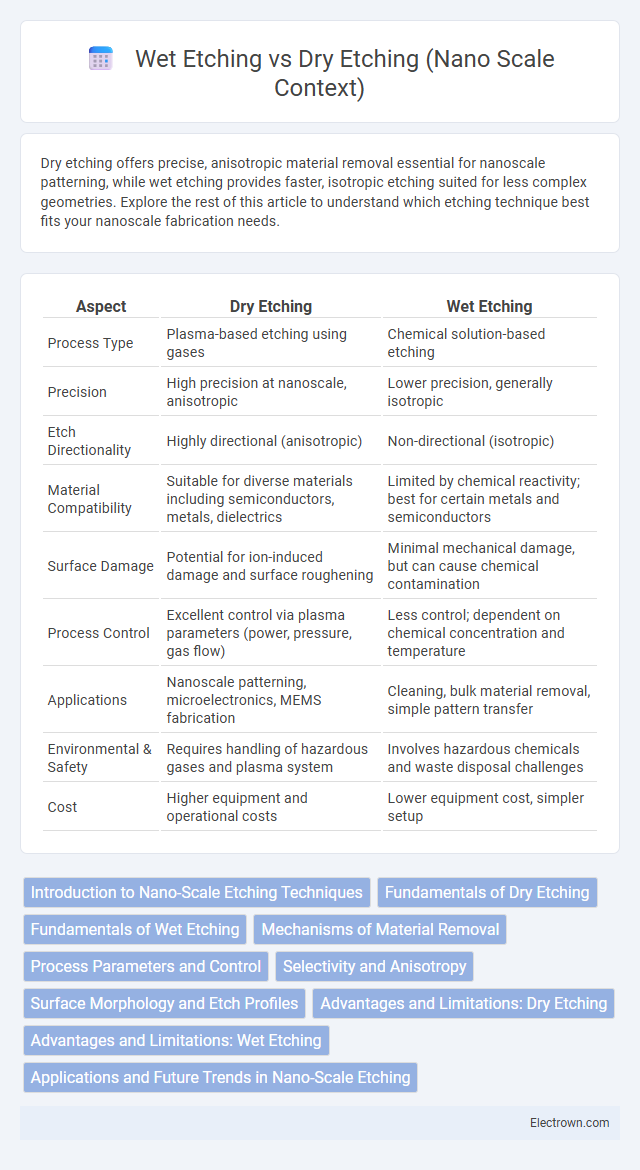
Dry etching offers precise, anisotropic material removal essential for nanoscale patterning, while wet etching provides faster, isotropic etching suited for less complex geometries. Explore the rest of this article to understand which etching technique best fits your nanoscale fabrication needs.
Table of Comparison
| Aspect | Dry Etching | Wet Etching |
|---|---|---|
| Process Type | Plasma-based etching using gases | Chemical solution-based etching |
| Precision | High precision at nanoscale, anisotropic | Lower precision, generally isotropic |
| Etch Directionality | Highly directional (anisotropic) | Non-directional (isotropic) |
| Material Compatibility | Suitable for diverse materials including semiconductors, metals, dielectrics | Limited by chemical reactivity; best for certain metals and semiconductors |
| Surface Damage | Potential for ion-induced damage and surface roughening | Minimal mechanical damage, but can cause chemical contamination |
| Process Control | Excellent control via plasma parameters (power, pressure, gas flow) | Less control; dependent on chemical concentration and temperature |
| Applications | Nanoscale patterning, microelectronics, MEMS fabrication | Cleaning, bulk material removal, simple pattern transfer |
| Environmental & Safety | Requires handling of hazardous gases and plasma system | Involves hazardous chemicals and waste disposal challenges |
| Cost | Higher equipment and operational costs | Lower equipment cost, simpler setup |
Introduction to Nano-Scale Etching Techniques
Nano-scale etching techniques are critical for fabricating semiconductor devices with high precision and minimal feature sizes. Dry etching employs plasma or reactive gases to selectively remove materials, offering superior anisotropy and control essential for creating intricate nanoscale patterns. Wet etching, utilizing chemical solutions, provides faster material removal but often results in less precise, isotropic etching, which can limit nanoscale resolution.
Fundamentals of Dry Etching
Dry etching at the nanoscale involves using plasma or reactive gases to precisely remove material via chemical reactions or physical sputtering, enabling superior anisotropy compared to wet etching. This technique allows for high-resolution patterning essential in semiconductor fabrication, maintaining structural integrity by minimizing undercutting. Your ability to control parameters like gas composition, power, and pressure is crucial for achieving precise etch depths and profiles in advanced nano-manufacturing.
Fundamentals of Wet Etching
Wet etching involves the chemical removal of material from a substrate using liquid etchants, which selectively dissolve specific layers at the nanoscale. This isotropic process affects the substrate uniformly in all directions, often resulting in undercutting beneath masking layers, making it challenging for precise nanoscale patterning. You should consider factors like etchant concentration, temperature, and etch rate to control the reaction and achieve desired feature dimensions in nanoscale fabrication.
Mechanisms of Material Removal
Dry etching removes material through plasma-generated reactive ions and radicals that chemically or physically disintegrate the surface at the nanoscale, enabling precise anisotropic patterning. Wet etching relies on liquid chemical solutions to selectively dissolve materials, often resulting in isotropic etching profiles due to uniform chemical attack from all directions. The distinct mechanisms in dry etching offer superior control over nanoscale feature shapes, while wet etching is generally simpler but less directionally selective.
Process Parameters and Control
Dry etching offers superior process parameters and control at the nanoscale due to its anisotropic etching behavior, precise gas flow regulation, and ability to finely tune plasma power, pressure, and etching time. Wet etching, while simpler, faces challenges in controlling etch uniformity and isotropy, often leading to undercutting and less precise feature definition on nanoscale devices. Your choice depends on the need for high-resolution, directional etching in advanced semiconductor fabrication, where dry etching provides enhanced process repeatability and dimensional accuracy.
Selectivity and Anisotropy
Dry etching offers superior anisotropy due to its directional ion bombardment, enabling precise pattern transfer essential at the nanoscale. Wet etching typically exhibits high selectivity but tends to be isotropic, causing lateral etching that compromises feature fidelity. Your choice between these methods depends on whether anisotropic profile control or material selectivity is the priority in your nanofabrication process.
Surface Morphology and Etch Profiles
Dry etching offers superior control over surface morphology and etch profiles at the nanoscale, enabling highly anisotropic and precise pattern transfer crucial for advanced semiconductor fabrication. In contrast, wet etching tends to produce isotropic profiles with less definable edges and can lead to surface roughness due to chemical undercutting. Your choice between dry and wet etching directly influences the fidelity and performance of nanoscale devices, making dry etching the preferred method for applications demanding sharp, vertical sidewalls and minimal surface damage.
Advantages and Limitations: Dry Etching
Dry etching offers superior anisotropy and precise control over etch profiles, essential for nanoscale fabrication and complex microstructures. It minimizes undercutting and contamination risks compared to wet etching, enhancing feature accuracy and repeatability. However, dry etching requires sophisticated equipment and can induce surface damage or residue buildup, potentially impacting your device's performance and necessitating careful process optimization.
Advantages and Limitations: Wet Etching
Wet etching offers high selectivity and cost-effectiveness for material removal at the nanoscale, particularly excelling in isotropic etching of silicon dioxide and other oxides. Limitations include undercutting due to isotropic nature, limited anisotropy control, and potential environmental hazards from chemical waste disposal. Precise process control is challenging, impacting the accuracy of nanoscale feature definition compared to dry etching methods.
Applications and Future Trends in Nano-Scale Etching
Dry etching, key for achieving high-precision patterns in semiconductor fabrication, excels in creating intricate nanoscale features used in advanced electronics and MEMS devices. Wet etching remains valuable for its cost-effectiveness and simplicity in applications like mask removal and certain biosensor fabrications requiring less stringent dimensional control. Future trends in nano-scale etching focus on hybrid techniques integrating dry and wet methods to balance precision and throughput, alongside advancements in plasma chemistries and atomic layer etching for enhanced control at atomic scales, empowering your next-generation nanodevices.
Dry Etching vs Wet Etching (nano scale context) Infographic