Nanoimprint Lithography offers high throughput and cost-effective patterning by physically stamping nanoscale features onto substrates, making it ideal for large-area applications. Electron Beam Lithography provides unparalleled resolution and flexibility for creating intricate designs at the nanoscale, though it is slower and more expensive; explore the rest of the article to determine which technology best suits Your nanofabrication needs.
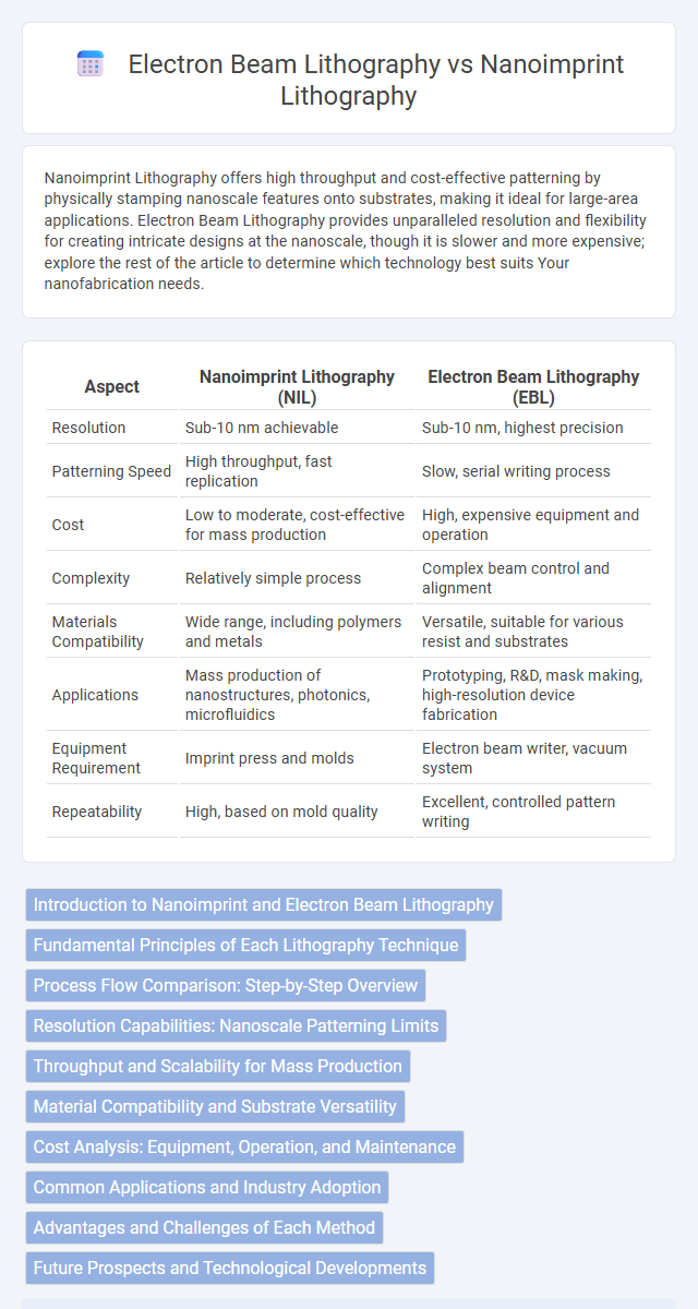
Table of Comparison
| Aspect | Nanoimprint Lithography (NIL) | Electron Beam Lithography (EBL) |
|---|---|---|
| Resolution | Sub-10 nm achievable | Sub-10 nm, highest precision |
| Patterning Speed | High throughput, fast replication | Slow, serial writing process |
| Cost | Low to moderate, cost-effective for mass production | High, expensive equipment and operation |
| Complexity | Relatively simple process | Complex beam control and alignment |
| Materials Compatibility | Wide range, including polymers and metals | Versatile, suitable for various resist and substrates |
| Applications | Mass production of nanostructures, photonics, microfluidics | Prototyping, R&D, mask making, high-resolution device fabrication |
| Equipment Requirement | Imprint press and molds | Electron beam writer, vacuum system |
| Repeatability | High, based on mold quality | Excellent, controlled pattern writing |
Introduction to Nanoimprint and Electron Beam Lithography
Nanoimprint Lithography (NIL) employs a physical embossing process to create nanoscale patterns by pressing a mold into a resist material, enabling high-throughput and cost-effective fabrication of nanostructures. Electron Beam Lithography (EBL) uses a focused electron beam to directly write complex patterns onto a resist, offering unmatched resolution and flexibility for prototype and research applications. Both techniques are pivotal in semiconductor manufacturing, with NIL excelling in volume production and EBL preferred for precision and versatility in micro- and nanofabrication.
Fundamental Principles of Each Lithography Technique
Nanoimprint Lithography (NIL) operates by mechanically pressing a patterned mold onto a resist-coated substrate to replicate nanoscale features through physical deformation and subsequent curing. Electron Beam Lithography (EBL) relies on a focused electron beam to directly write patterns by altering the chemical solubility of a resist, enabling high-resolution pattern definition without masks. Both techniques offer nanoscale precision, with NIL excelling in high-throughput replication and EBL providing unmatched flexibility for complex, customizable designs.
Process Flow Comparison: Step-by-Step Overview
Nanoimprint Lithography (NIL) involves creating nanoscale patterns by mechanically deforming a resist layer with a mold, followed by curing and pattern transfer, making it efficient for high-throughput replication. Electron Beam Lithography (EBL) uses a focused electron beam to directly write patterns onto a resist, enabling high-resolution and flexible design but with slower exposure times and complex resist processing. NIL's process flow includes mold fabrication, resist coating, imprinting, curing, and mold release, whereas EBL requires resist coating, electron beam exposure, development, and often subsequent etching for pattern transfer.
Resolution Capabilities: Nanoscale Patterning Limits
Nanoimprint Lithography (NIL) typically achieves resolution capabilities down to 5-10 nanometers by directly imprinting patterns using a physical mold, enabling high throughput nanoscale patterning ideal for large-area fabrication. Electron Beam Lithography (EBL), on the other hand, offers superior resolution reaching sub-10 nanometer features through precise electron beam exposure but suffers from slower writing speeds, making it better suited for prototyping and low-volume production. Both technologies push the boundaries of nanoscale patterning, with NIL favoring scalability and EBL excelling in ultra-high resolution detail.
Throughput and Scalability for Mass Production
Nanoimprint Lithography (NIL) offers significantly higher throughput and better scalability for mass production compared to Electron Beam Lithography (EBL) due to its parallel patterning capability and ability to replicate nanoscale features rapidly across large areas. EBL, while providing unmatched resolution and flexibility for complex designs, suffers from inherently slow serial writing processes, making it less suitable for high-volume manufacturing. Consequently, NIL is preferred in industries requiring efficient large-scale fabrication of nanostructures, such as semiconductor manufacturing and flexible electronics.
Material Compatibility and Substrate Versatility
Nanoimprint Lithography (NIL) offers superior material compatibility by enabling patterning on a diverse range of polymers, resists, and flexible substrates, making it ideal for flexible electronics and soft materials. Electron Beam Lithography (EBL) excels in high-resolution patterning but is limited by substrate charging effects, requiring conductive or specially coated substrates primarily in semiconductor and metal films. NIL's versatility in processing large-area, non-planar, and curved substrates contrasts with EBL's suitability for rigid, planar substrates demanding nanoscale precision.
Cost Analysis: Equipment, Operation, and Maintenance
Nanoimprint Lithography (NIL) offers significantly lower equipment and operational costs compared to Electron Beam Lithography (EBL), making it more cost-effective for high-volume production. EBL requires expensive, high-precision electron beam systems and complex maintenance routines, driving up long-term operational expenses. Your choice between NIL and EBL will depend on balancing initial investment against throughput needs and maintenance budgets.
Common Applications and Industry Adoption
Nanoimprint Lithography (NIL) is widely adopted in the production of nanoscale patterns for applications such as flexible electronics, nanophotonic devices, and high-density data storage due to its high throughput and cost-effectiveness. Electron Beam Lithography (EBL) remains the preferred method for research and development environments and prototyping in semiconductor manufacturing because of its superior resolution and patterning precision at the nanometer scale. While NIL dominates in industries requiring mass production like optical components and MEMS, EBL is extensively utilized in academia and specialized industries focused on advanced quantum devices and novel material studies.
Advantages and Challenges of Each Method
Nanoimprint Lithography offers high throughput and cost-effectiveness with the ability to produce nanoscale patterns over large areas, making it ideal for mass production. However, challenges include mold fabrication complexity and potential defects during the imprint process. Electron Beam Lithography provides unparalleled resolution and patterning flexibility for custom designs, but its slow writing speed and high equipment costs limit scalability for high-volume manufacturing.
Future Prospects and Technological Developments
Nanoimprint Lithography (NIL) offers promising future prospects due to its high throughput and low cost, making it ideal for large-area nanoscale patterning compared to Electron Beam Lithography (EBL), which excels in ultra-high resolution but remains limited by slower processing speeds and higher costs. Advances in NIL materials and template fabrication technologies are expected to enhance pattern fidelity and durability, expanding its application in flexible electronics and photonics. Your choice between NIL and EBL should consider emerging developments such as hybrid lithography techniques that combine EBL's precision with NIL's scalability to meet evolving industry demands.
Nanoimprint Lithography vs Electron Beam Lithography Infographic