Epitaxial growth ensures a highly ordered atomic alignment by depositing a crystalline layer on a substrate with matching lattice structures, promoting superior electronic and optical properties. Van der Waals growth, on the other hand, relies on weak intermolecular forces to stack layered materials without strict lattice matching, enabling flexible heterostructures and novel device applications; explore the article to understand which method suits your material engineering needs best.
Table of Comparison
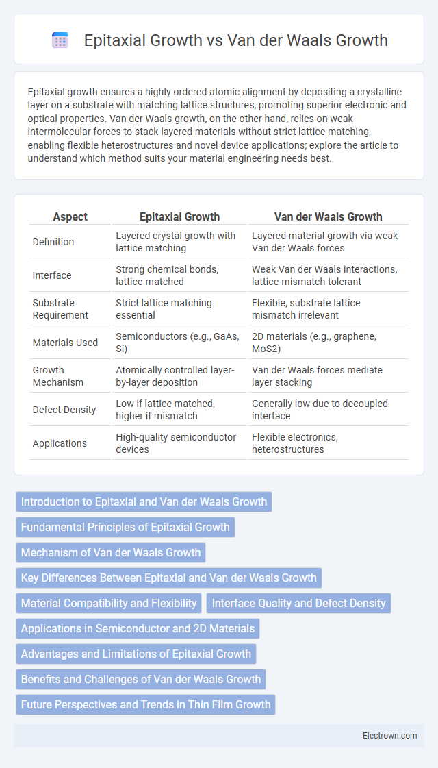
| Aspect | Epitaxial Growth | Van der Waals Growth |
|---|---|---|
| Definition | Layered crystal growth with lattice matching | Layered material growth via weak Van der Waals forces |
| Interface | Strong chemical bonds, lattice-matched | Weak Van der Waals interactions, lattice-mismatch tolerant |
| Substrate Requirement | Strict lattice matching essential | Flexible, substrate lattice mismatch irrelevant |
| Materials Used | Semiconductors (e.g., GaAs, Si) | 2D materials (e.g., graphene, MoS2) |
| Growth Mechanism | Atomically controlled layer-by-layer deposition | Van der Waals forces mediate layer stacking |
| Defect Density | Low if lattice matched, higher if mismatch | Generally low due to decoupled interface |
| Applications | High-quality semiconductor devices | Flexible electronics, heterostructures |
Introduction to Epitaxial and Van der Waals Growth
Epitaxial growth involves the deposition of a crystalline layer on a substrate with a matching lattice structure, enabling precise control over film quality and orientation, essential for semiconductor device fabrication. Van der Waals growth, by contrast, relies on weak interlayer forces to assemble layered materials without strict lattice matching, facilitating the production of heterostructures with diverse compositions and minimal strain. Understanding these distinct mechanisms allows you to select the optimal growth method for applications ranging from microelectronics to advanced nanomaterials.
Fundamental Principles of Epitaxial Growth
Epitaxial growth involves the deposition of a crystalline layer on a substrate, where the deposited crystal adopts the lattice structure and orientation of the underlying material due to strong chemical bonding and lattice matching. This process relies on atom-by-atom alignment, ensuring coherent interfaces and minimal defects, critical for high-quality film fabrication in semiconductors and optoelectronics. In contrast, Van der Waals growth leverages weak van der Waals forces between layers, allowing for stacking of lattice-mismatched materials without epitaxial constraints.
Mechanism of Van der Waals Growth
Van der Waals growth operates by weakly bonding layered materials through van der Waals forces, allowing for the assembly of heterostructures without strict lattice matching. This mechanism enables the stacking of two-dimensional materials with atomically sharp interfaces and minimal strain. Unlike epitaxial growth, which relies on covalent bonding and lattice alignment, van der Waals growth facilitates greater flexibility in creating novel structures with diverse electronic and optical properties.
Key Differences Between Epitaxial and Van der Waals Growth
Epitaxial growth involves the deposition of a crystalline layer on a substrate with a matching lattice structure, enabling strong atomic bonding and alignment, while Van der Waals growth relies on weak interlayer Van der Waals forces without requiring lattice matching. Epitaxial growth typically requires stringent substrate compatibility and high-temperature conditions, whereas Van der Waals growth allows for the stacking of disparate two-dimensional materials with greater flexibility and lower thermal budgets. These fundamental differences influence material quality, interface properties, and potential applications in semiconductor and layered material technologies.
Material Compatibility and Flexibility
Epitaxial growth requires strict lattice matching between the substrate and the grown layer, limiting material compatibility to closely related crystals and reducing flexibility in device design. Van der Waals growth allows for the stacking of dissimilar materials without lattice matching constraints, providing greater flexibility and enabling heterostructures with diverse material combinations. Your choice between these methods impacts the integration of novel materials and the performance of advanced electronic and optoelectronic devices.
Interface Quality and Defect Density
Epitaxial growth typically yields high interface quality with strong atomic bonding and low defect density due to lattice matching between substrate and film, enabling coherent crystal structures. Van der Waals growth exploits weak interlayer forces allowing deposition on diverse substrates with reduced strain, yet it often results in higher defect density and less ideal interface quality because of weaker adhesion and potential misalignment. Optimizing epitaxial growth parameters enhances crystalline perfection, while advances in Van der Waals techniques aim to minimize defects across heterostructures in emerging two-dimensional materials.
Applications in Semiconductor and 2D Materials
Epitaxial growth enables precise layering of semiconductor crystals, crucial for fabricating high-performance devices like LEDs, lasers, and transistors with well-defined electronic properties. Van der Waals growth facilitates the assembly of 2D materials, such as graphene and transition metal dichalcogenides, allowing for flexible and ultra-thin electronic applications including sensors and flexible displays. Your choice between these methods depends on the required material integration and the desired device architecture in advanced semiconductor and 2D material applications.
Advantages and Limitations of Epitaxial Growth
Epitaxial growth offers precise control over crystal orientation and thickness, enabling high-quality semiconductor layers essential for advanced electronic and optoelectronic devices. Its primary advantage lies in producing defect-minimized interfaces, which improve device performance and efficiency. However, epitaxial growth requires expensive substrates and strict lattice matching, limiting material compatibility and increasing production costs in Your fabrication processes.
Benefits and Challenges of Van der Waals Growth
Van der Waals growth offers unique benefits such as the ability to stack diverse two-dimensional materials without lattice matching constraints, enabling the integration of novel heterostructures with tailored electronic and optical properties. However, challenges include controlling layer uniformity and interface quality due to weak interlayer forces, which can impact device performance and reproducibility. Your success in utilizing Van der Waals growth depends on precise control of growth conditions and advanced characterization techniques to overcome these limitations.
Future Perspectives and Trends in Thin Film Growth
Epitaxial growth techniques continue to evolve with advancements in atomic layer precision and in-situ monitoring, driving the development of ultra-high-quality epitaxial films for next-generation semiconductors and optoelectronic devices. Van der Waals growth offers promising future perspectives by enabling the integration of diverse 2D materials without lattice matching constraints, facilitating novel heterostructures with tailored electronic and optical properties. Emerging trends emphasize hybrid approaches combining epitaxial and Van der Waals methods to harness the benefits of both techniques for scalable, defect-free thin film fabrication in flexible electronics and quantum computing applications.
Epitaxial growth vs Van der Waals growth Infographic