Electrostatic doping modulates charge carrier density in materials using an external electric field without introducing impurities, preserving the intrinsic lattice structure, whereas chemical doping involves adding foreign atoms or molecules to alter electrical properties permanently. Discover how these doping methods impact device performance and which suits Your applications best by reading the full article.
Table of Comparison
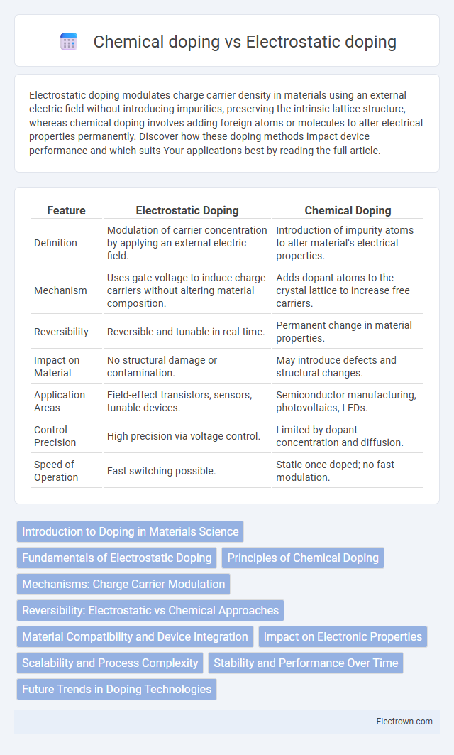
| Feature | Electrostatic Doping | Chemical Doping |
|---|---|---|
| Definition | Modulation of carrier concentration by applying an external electric field. | Introduction of impurity atoms to alter material's electrical properties. |
| Mechanism | Uses gate voltage to induce charge carriers without altering material composition. | Adds dopant atoms to the crystal lattice to increase free carriers. |
| Reversibility | Reversible and tunable in real-time. | Permanent change in material properties. |
| Impact on Material | No structural damage or contamination. | May introduce defects and structural changes. |
| Application Areas | Field-effect transistors, sensors, tunable devices. | Semiconductor manufacturing, photovoltaics, LEDs. |
| Control Precision | High precision via voltage control. | Limited by dopant concentration and diffusion. |
| Speed of Operation | Fast switching possible. | Static once doped; no fast modulation. |
Introduction to Doping in Materials Science
Doping in materials science involves intentionally introducing impurities to alter the electrical properties of semiconductors, enabling precise control of conductivity and device performance. Electrostatic doping uses external electric fields to induce charge carriers without altering the material's chemical composition, offering reversible and tunable modulation. Chemical doping incorporates impurity atoms or molecules directly into the material lattice, creating permanent changes in carrier concentration and enabling stable, long-term conductivity adjustments.
Fundamentals of Electrostatic Doping
Electrostatic doping involves modulating the charge carrier concentration in a semiconductor by applying an external electric field, enabling reversible control without altering the material's chemical composition. This method relies on field-effect principles, where an electric field induces charge accumulation or depletion at the semiconductor interface, effectively changing its conductivity. Your devices benefit from precise, tunable doping levels, unlike chemical doping that permanently introduces impurities into the lattice.
Principles of Chemical Doping
Chemical doping involves introducing impurity atoms or molecules into a semiconductor material to alter its electrical properties by creating free charge carriers. This process changes the intrinsic conductivity by adding donor or acceptor atoms that either donate electrons or create holes in the host lattice. The effectiveness of chemical doping depends on factors such as dopant concentration, activation energy, and the interaction between dopant and host atoms.
Mechanisms: Charge Carrier Modulation
Electrostatic doping modulates charge carriers by applying an external electric field, which induces charge accumulation or depletion at the material's surface without altering its chemical composition. Chemical doping introduces impurities or dopant atoms into the semiconductor lattice, creating permanent charge carriers by donating or accepting electrons. Your choice between these mechanisms affects device performance, as electrostatic doping enables reversible and tunable carrier densities, while chemical doping imparts fixed, often less controllable charge levels.
Reversibility: Electrostatic vs Chemical Approaches
Electrostatic doping offers reversible modulation of carrier concentration by applying an external electric field, allowing for dynamic control without permanent alteration of the material's structure. Chemical doping introduces impurities into the semiconductor lattice, resulting in permanent changes that cannot be undone without additional processing. This reversibility in electrostatic doping makes it highly suitable for applications requiring real-time tunability, such as field-effect transistors and sensors.
Material Compatibility and Device Integration
Electrostatic doping offers superior material compatibility by enabling reversible and non-destructive modulation of carrier densities in diverse materials such as graphene and transition metal dichalcogenides, without altering their intrinsic properties. Chemical doping introduces impurities that may compromise device stability and complicate integration due to permanent lattice disruptions and uncontrolled dopant diffusion. Your device integration benefits from electrostatic doping's precise control and cleaner interfaces, essential for next-generation flexible and nanoscale electronics.
Impact on Electronic Properties
Electrostatic doping modulates electronic properties by inducing charge carriers through an external electric field without altering the material's lattice structure, preserving high carrier mobility and reversible control over conductivity. Chemical doping introduces impurity atoms into the crystal lattice, causing permanent changes that can enhance carrier concentration but often reduce mobility due to increased scattering and defects. Understanding these differences helps you tailor electronic device performance by balancing stability and tunability.
Scalability and Process Complexity
Electrostatic doping offers superior scalability with precise, reversible control of carrier concentration, making it ideal for nanoscale and flexible electronics, while chemical doping involves permanent changes that can limit device miniaturization. The process complexity of electrostatic doping is lower due to its clean, solution-free approach without introducing impurities, whereas chemical doping requires intricate synthesis steps and careful control of dopant distribution. Electrostatic doping also facilitates rapid prototyping and device tuning, contrasting the time-consuming annealing and activation processes typical of chemical doping.
Stability and Performance Over Time
Electrostatic doping offers superior stability over time due to its reversible and non-destructive nature, avoiding permanent alterations to the material's lattice structure. Chemical doping can introduce defects and impurities that degrade device performance and reliability through chemical reactions and diffusion processes. Performance degradation in chemically doped materials often results from dopant diffusion and defect generation, while electrostatic doping maintains consistent carrier concentration, enhancing long-term operational stability.
Future Trends in Doping Technologies
Future trends in doping technologies emphasize the development of electrostatic doping due to its precision and reversibility, enabling dynamic control of carrier concentration in semiconductor devices. Advances in nanomaterials and two-dimensional semiconductors are propelling electrostatic doping towards more scalable and energy-efficient applications compared to traditional chemical doping methods. The integration of machine learning algorithms with doping processes is also driving innovations, optimizing doping profiles for enhanced device performance in next-generation electronics.
Electrostatic doping vs Chemical doping Infographic