Heterojunctions in nanostructures involve interfaces between different semiconductor materials, creating unique electronic and optical properties essential for advanced device performance, while homojunctions consist of the same material with varied doping, offering simpler charge carrier dynamics. Explore the detailed comparison to understand how each junction impacts your nanodevice applications and optimizes functionality.
Table of Comparison
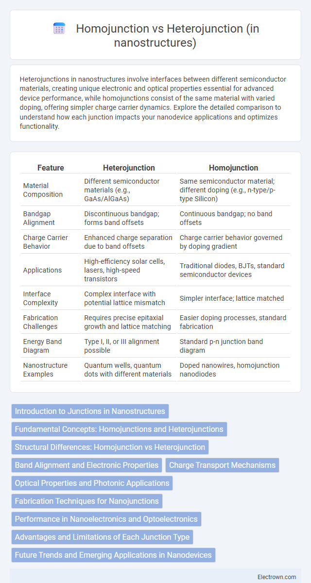
| Feature | Heterojunction | Homojunction |
|---|---|---|
| Material Composition | Different semiconductor materials (e.g., GaAs/AlGaAs) | Same semiconductor material; different doping (e.g., n-type/p-type Silicon) |
| Bandgap Alignment | Discontinuous bandgap; forms band offsets | Continuous bandgap; no band offsets |
| Charge Carrier Behavior | Enhanced charge separation due to band offsets | Charge carrier behavior governed by doping gradient |
| Applications | High-efficiency solar cells, lasers, high-speed transistors | Traditional diodes, BJTs, standard semiconductor devices |
| Interface Complexity | Complex interface with potential lattice mismatch | Simpler interface; lattice matched |
| Fabrication Challenges | Requires precise epitaxial growth and lattice matching | Easier doping processes, standard fabrication |
| Energy Band Diagram | Type I, II, or III alignment possible | Standard p-n junction band diagram |
| Nanostructure Examples | Quantum wells, quantum dots with different materials | Doped nanowires, homojunction nanodiodes |
Introduction to Junctions in Nanostructures
Nanostructure junctions form critical interfaces where two semiconductor materials meet, influencing electronic and optical properties at the nanoscale. Homojunctions consist of the same semiconductor material with varying doping levels, enabling charge carrier control within a single bandgap system. Heterojunctions combine different semiconductor materials with distinct bandgaps, creating unique energy barriers that enhance device performance in applications like quantum wells and nanoscale transistors.
Fundamental Concepts: Homojunctions and Heterojunctions
Homojunctions in nanostructures consist of an interface between two regions of the same semiconductor material with different doping types, enabling charge carrier separation through band bending. Heterojunctions form at the interface of two distinct semiconductors with different bandgaps and electron affinities, creating discontinuities in conduction and valence bands that enhance charge carrier dynamics. These fundamental differences influence electron transport, recombination rates, and device performance in nanoscale electronics and optoelectronics.
Structural Differences: Homojunction vs Heterojunction
Homojunction nanostructures are formed by joining two regions of the same semiconductor material with identical bandgaps, resulting in a uniform crystal lattice and consistent electronic properties across the junction. In contrast, heterojunction nanostructures involve the interface between two different semiconductor materials with varying bandgaps and lattice constants, creating distinct energy band alignments and potential barriers that influence charge carrier behavior. Understanding these structural differences is crucial for tailoring electronic and optoelectronic device performance, enabling your designs to optimize charge transport and recombination efficiency.
Band Alignment and Electronic Properties
Heterojunctions in nanostructures exhibit band alignment characterized by staggered or straddling configurations, enabling efficient charge separation and tailored electronic properties, while homojunctions feature uniform band gaps with more straightforward electron flow. The differing band offsets in heterojunctions create potential wells or barriers, crucial for designing high-performance optoelectronic devices. Understanding these variations allows you to optimize nanodevice functionality by selecting junction types that suit specific electronic and transport requirements.
Charge Transport Mechanisms
Charge transport in heterojunction nanostructures occurs primarily through band offset-driven tunneling and thermionic emission across the interface between two materials with different bandgaps, enhancing carrier separation and reducing recombination. In homojunction nanostructures, charge transport relies on diffusion and drift mechanisms within a single material, with recombination dynamics largely influenced by uniform band alignment and defect states. The distinct band alignments in heterojunctions create potential barriers that modulate carrier mobility and lead to improved device performance in applications like photovoltaics and nanoelectronics.
Optical Properties and Photonic Applications
Heterojunctions in nanostructures exhibit enhanced optical properties such as improved charge separation and broader absorption spectra compared to homojunctions, which typically feature uniform bandgaps. These characteristics make heterojunctions highly suitable for photonic applications like solar cells, LEDs, and photodetectors, where efficient light manipulation and carrier dynamics are critical. Your choice of junction type directly influences device performance, particularly in tailoring optical responses for advanced nanophotonic technologies.
Fabrication Techniques for Nanojunctions
Fabrication techniques for heterojunction nanostructures often involve molecular beam epitaxy (MBE) and chemical vapor deposition (CVD), enabling precise control over material interfaces and band alignment at the nanoscale. Homojunction nanostructures typically utilize methods like doping modulation and ion implantation within a single semiconductor material to create distinct regions with varied electrical properties. Your choice between these nanojunctions depends on the required electronic or optoelectronic performance, as fabrication intricacies directly impact device efficiency and functionality.
Performance in Nanoelectronics and Optoelectronics
Heterojunctions in nanostructures exhibit superior performance in nanoelectronics and optoelectronics due to their ability to create energy band offsets that enhance charge carrier separation and minimize recombination losses. Homojunctions, composed of the same semiconductor material, typically suffer from limited bandgap engineering and reduced efficiency in device applications like photodetectors and transistors. Leveraging heterojunctions can significantly improve your device's electron mobility, tunneling efficiency, and light emission properties, making them preferable for advanced nanoscale technology.
Advantages and Limitations of Each Junction Type
Heterojunctions in nanostructures offer superior electronic and optical properties due to the interface between different semiconductor materials, enabling enhanced charge separation and tailored band alignments crucial for high-efficiency devices like solar cells and LEDs. However, lattice mismatch and interface defects can introduce recombination centers, limiting device performance and fabrication scalability. Homojunctions provide simpler fabrication with better lattice matching and fewer interface states, resulting in more stable electrical characteristics but lack the bandgap engineering versatility and efficiency improvements offered by heterojunctions.
Future Trends and Emerging Applications in Nanodevices
Heterojunctions in nanostructures offer superior electronic and optoelectronic performance due to their ability to combine materials with differing bandgaps, enabling tailored charge carrier dynamics crucial for next-generation nanodevices. Future trends point towards integrating heterojunctions in quantum dot lasers, high-efficiency photovoltaics, and ultra-fast transistors, leveraging their enhanced carrier mobility and reduced recombination rates. Your choice between heterojunction and homojunction architectures will significantly impact device scalability and functionality in emerging applications such as flexible electronics and nanoscale sensors.
Heterojunction vs Homojunction (in nanostructures) Infographic