Top-gate and bottom-gate architectures differ primarily in their gate electrode positioning relative to the semiconductor channel, impacting device performance such as charge carrier mobility and gate control at the nanoscale. Understanding these distinctions can help optimize your nanoscale transistor design; explore the rest of the article to uncover detailed comparisons and practical implications.
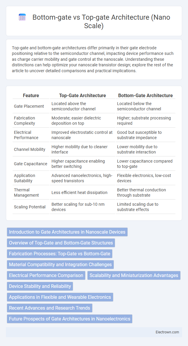
Table of Comparison
| Feature | Top-Gate Architecture | Bottom-Gate Architecture |
|---|---|---|
| Gate Placement | Located above the semiconductor channel | Located below the semiconductor channel |
| Fabrication Complexity | Moderate; easier dielectric deposition on top | Higher; substrate processing required |
| Electrical Performance | Improved electrostatic control at nanoscale | Good but susceptible to substrate impedance |
| Channel Mobility | Higher mobility due to cleaner interface | Lower mobility due to substrate interaction |
| Gate Capacitance | Higher capacitance enabling better switching | Lower capacitance compared to top-gate |
| Application Suitability | Advanced nanoelectronics, high-speed transistors | Flexible electronics, low-cost devices |
| Thermal Management | Less efficient heat dissipation | Better thermal conduction through substrate |
| Scaling Potential | Better scaling for sub-10 nm devices | Limited scaling due to substrate effects |
Introduction to Gate Architectures in Nanoscale Devices
Top-gate and bottom-gate architectures are fundamental designs in nanoscale transistors, influencing device performance, scalability, and electrical characteristics. Top-gate structures position the gate electrode above the semiconductor channel, enabling superior electrostatic control and reduced short-channel effects, while bottom-gate architectures place the gate beneath the channel, often facilitating simpler fabrication and better substrate compatibility. Understanding the distinction between these gate placements is crucial for optimizing your nanoscale device's switching speed, power efficiency, and overall integration in advanced electronic circuits.
Overview of Top-Gate and Bottom-Gate Structures
Top-gate and bottom-gate architectures differ primarily in the placement of the gate electrode relative to the semiconductor channel in nanoscale devices. In top-gate structures, the gate electrode is positioned above the active semiconductor layer, allowing for better electrostatic control and reduced short-channel effects. Bottom-gate designs place the gate electrode below the semiconductor, often resulting in simpler fabrication and improved compatibility with certain substrates but can suffer from weaker gate coupling at reduced channel lengths.
Fabrication Processes: Top-Gate vs Bottom-Gate
Top-gate architecture fabrication involves depositing the gate electrode after forming the semiconductor layer, allowing precise control over the gate dielectric and minimizing interface traps, which enhances device performance at the nanoscale. Bottom-gate fabrication starts with the gate electrode and dielectric layers on the substrate, followed by semiconductor deposition, offering simpler processing but potentially higher interface defect densities. Your choice between top-gate and bottom-gate structures impacts fabrication complexity, scalability, and electrical characteristics in nanoscale devices.
Material Compatibility and Integration Challenges
Top-gate architecture offers enhanced material compatibility with high-k dielectrics and metals, facilitating superior electrostatic control at the nanoscale. Bottom-gate structures often face challenges integrating with flexible substrates due to thermal budget constraints and interface quality issues. Integration hurdles in bottom-gate designs are exacerbated by the need for precise alignment and complex interlayer dielectric deposition, impacting device scalability and performance.
Electrical Performance Comparison
Top-gate architecture provides superior electrical performance at the nanoscale due to enhanced gate control, resulting in reduced short-channel effects and improved subthreshold slope. Bottom-gate structures often suffer from increased parasitic capacitance and weaker electrostatic control, which can degrade carrier mobility and drive current. Choosing the appropriate design impacts your device's switching speed, power efficiency, and overall reliability in nanoelectronic applications.
Scalability and Miniaturization Advantages
Top-gate architecture offers superior scalability by allowing precise control over the channel with a shorter gate length, enhancing device performance at the nanoscale. Bottom-gate designs provide easier fabrication on large substrates but face challenges in further miniaturization due to increased parasitic capacitance and reduced electrostatic control. Your choice of top-gate devices enables more effective miniaturization and integration in ultra-scaled nanoelectronic applications.
Device Stability and Reliability
Top-gate architecture in nanoscale devices offers enhanced device stability and reliability due to better electrostatic control and reduced interface trap density compared to bottom-gate structures. The closer proximity of the gate electrode to the channel in top-gate designs minimizes short-channel effects and improves charge carrier mobility, thereby enhancing operational consistency. In contrast, bottom-gate devices often suffer from greater susceptibility to threshold voltage shifts and increased leakage currents, which negatively impact long-term device performance.
Applications in Flexible and Wearable Electronics
Top-gate and bottom-gate architectures at the nanoscale influence the performance and integration of flexible and wearable electronics by determining device stability and electrical characteristics. Top-gate designs offer enhanced protection of the semiconductor layer, improving device durability under mechanical stress, which is critical for wearable sensors and flexible displays. Bottom-gate configurations enable simpler fabrication on flexible substrates, promoting cost-effective large-area electronics essential for wearable health monitoring systems.
Recent Advances and Research Trends
Recent advances in nano-scale transistor design have highlighted significant improvements in both top-gate and bottom-gate architectures, with top-gate devices demonstrating enhanced electrostatic control and reduced short-channel effects. Research trends focus on integrating high-k dielectrics and novel 2D materials like transition metal dichalcogenides (TMDCs) to optimize carrier mobility and minimize leakage currents in bottom-gate configurations. Experimental results reveal that hybrid gate structures combining top- and bottom-gate features offer promising pathways for scalable, high-performance nanoelectronics with improved reliability and lower power consumption.
Future Prospects of Gate Architectures in Nanoelectronics
Top-gate and bottom-gate architectures each offer unique advantages in nanoelectronics, influencing device scaling, performance, and integration density. Top-gate structures provide superior electrostatic control and reduced short-channel effects, while bottom-gate designs facilitate easier fabrication and better interface quality in certain materials. Future prospects hinge on optimizing these architectures for emerging 3D integration and flexible electronics, where balancing gate control and manufacturability will be critical for advancing your nano-scale device capabilities.
Top-gate vs Bottom-gate architecture (nano scale) Infographic