Vertical nanotube arrays provide superior surface area and enhanced electron transport, making them ideal for sensors and energy storage devices, while horizontal nanotube arrays offer better mechanical flexibility and ease of integration into electronic circuits. Explore the detailed advantages and applications of each to understand which nanotube orientation best suits Your technological needs.
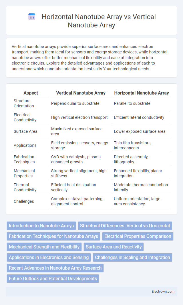
Table of Comparison
| Aspect | Vertical Nanotube Array | Horizontal Nanotube Array |
|---|---|---|
| Structure Orientation | Perpendicular to substrate | Parallel to substrate |
| Electrical Conductivity | High vertical electron transport | Efficient lateral conductivity |
| Surface Area | Maximized exposed surface area | Lower exposed surface area |
| Applications | Field emission, sensors, energy storage | Thin-film transistors, interconnects |
| Fabrication Techniques | CVD with catalysts, plasma-enhanced growth | Directed assembly, lithography |
| Mechanical Properties | Strong vertical alignment, high stiffness | Enhanced flexibility, planar integration |
| Thermal Conductivity | Efficient heat dissipation vertically | Moderate thermal conduction laterally |
| Challenges | Complex catalyst patterning, alignment control | Uniform orientation, large-area consistency |
Introduction to Nanotube Arrays
Nanotube arrays consist of vertically or horizontally aligned carbon nanotubes grown on substrates, offering distinct structural and functional properties. Vertical nanotube arrays exhibit high surface area and superior electron transport, ideal for sensors and energy storage applications. Horizontal nanotube arrays provide enhanced mechanical flexibility and conductivity, suited for flexible electronics and interconnects.
Structural Differences: Vertical vs Horizontal
Vertical nanotube arrays feature carbon nanotubes aligned perpendicular to the substrate, providing high surface area and efficient electron transport pathways ideal for sensors and field emission devices. Horizontal nanotube arrays consist of nanotubes laid parallel to the substrate, offering enhanced electrical conductivity along the surface and better mechanical flexibility for flexible electronics. Your choice between vertical and horizontal configurations impacts device performance based on alignment-dependent properties like electron mobility and surface interactions.
Fabrication Techniques for Nanotube Arrays
Vertical nanotube arrays are commonly fabricated using chemical vapor deposition (CVD) methods, where nanotubes grow perpendicular to the substrate, enabling high-density and uniform structures. Horizontal nanotube arrays often require transfer techniques or specialized alignment processes such as Langmuir-Blodgett assembly or shear force alignment to achieve controlled orientation on flat surfaces. Your choice of fabrication technique impacts the mechanical, electrical, and optical properties, making it crucial to select a method aligned with your device application requirements.
Electrical Properties Comparison
Vertical nanotube arrays exhibit superior electrical conductivity due to their aligned structure, which enables efficient electron transport along the nanotube's length. Horizontal nanotube arrays often suffer from increased electron scattering and resistance caused by tube-to-tube junctions and misalignment. Consequently, vertical configurations are preferred for high-performance applications requiring low-resistance pathways and enhanced charge carrier mobility.
Mechanical Strength and Flexibility
Vertical nanotube arrays exhibit superior mechanical strength due to their aligned structure, which effectively distributes stress and resists deformation under load. Horizontal nanotube arrays offer enhanced flexibility, allowing bending and twisting without breaking, making them ideal for applications requiring dynamic movement. Your choice between these structures depends on whether mechanical strength or flexibility is prioritized in the specific nanotechnology application.
Surface Area and Reactivity
Vertical nanotube arrays provide a significantly higher surface area than horizontal nanotube arrays due to their perpendicular orientation, which maximizes exposure to the surrounding environment. This increased surface area enhances reactivity, making vertical arrays more effective for applications like catalysis and sensing. Your choice between vertical and horizontal arrays should consider the desired interaction efficiency, with vertical arrays offering superior performance in surface-dependent reactions.
Applications in Electronics and Sensing
Vertical nanotube arrays provide enhanced electron transport and higher surface area, making them ideal for field-effect transistors, sensors, and energy storage devices. Horizontal nanotube arrays enable better integration with planar substrates, suitable for flexible electronics and transparent conductive films. Both configurations exhibit unique electrical, mechanical, and sensing properties tailored to specific applications in nanoelectronics and chemical or biological sensors.
Challenges in Scaling and Integration
Vertical nanotube arrays face challenges in uniformity and alignment control during large-scale fabrication, complicating integration with existing semiconductor processes. Horizontal nanotube arrays encounter difficulties in precise placement and consistent orientation on substrates, which limits scalable manufacturing and device yield. Optimizing your choice requires balancing these integration hurdles with the specific performance requirements of nanodevice applications.
Recent Advances in Nanotube Array Research
Recent advances in nanotube array research highlight significant differences between vertical and horizontal configurations in applications such as energy storage, sensing, and electronics. Vertical nanotube arrays demonstrate superior electron transport and surface area, enhancing performance in supercapacitors and photovoltaic devices, while horizontal nanotube arrays offer improved mechanical flexibility and easier integration into flexible electronics. Emerging fabrication techniques like chemical vapor deposition and template-assisted growth have enabled precise control over array orientation, density, and uniformity, driving innovations in nanodevices with tailored properties.
Future Outlook and Potential Developments
Vertical nanotube arrays offer superior electron transport and higher surface area, driving innovations in energy storage and sensors. Horizontal nanotube arrays provide enhanced mechanical flexibility and integration potential for flexible electronics and transparent conductive films. Your choice between these configurations will influence future device performance and scalability in emerging nanotechnology applications.
Vertical Nanotube Array vs Horizontal Nanotube Array Infographic