Hybrid perovskites offer superior optoelectronic properties and easier solution processing, making them attractive for flexible nanoelectronic devices, whereas inorganic perovskites provide enhanced thermal stability and longer operational lifetimes suitable for high-performance applications. Explore the rest of the article to understand how your choice between these materials can impact device efficiency and durability in nanoelectronics.
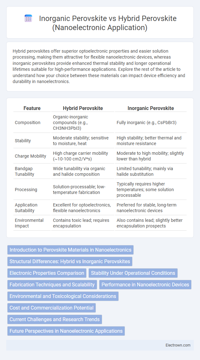
Table of Comparison
| Feature | Hybrid Perovskite | Inorganic Perovskite |
|---|---|---|
| Composition | Organic-inorganic compounds (e.g., CH3NH3PbI3) | Fully inorganic (e.g., CsPbBr3) |
| Stability | Moderate stability; sensitive to moisture, heat | High stability; better thermal and moisture resistance |
| Charge Mobility | High charge carrier mobility (~10-100 cm2/V*s) | Moderate to high mobility; slightly lower than hybrid |
| Bandgap Tunability | Wide tunability via organic and halide composition | Limited tunability; mainly via halide substitution |
| Processing | Solution-processable; low-temperature fabrication | Typically requires higher temperatures; some solution processable |
| Application Suitability | Excellent for optoelectronics, flexible nanoelectronics | Preferred for stable, long-term nanoelectronic devices |
| Environmental Impact | Contains toxic lead; requires encapsulation | Also contains lead; slightly better encapsulation prospects |
Introduction to Perovskite Materials in Nanoelectronics
Perovskite materials, characterized by the ABX3 crystal structure, have emerged as pivotal components in nanoelectronic devices due to their exceptional optoelectronic properties and tunable electronic bandgaps. Hybrid perovskites, typically composed of organic-inorganic components such as methylammonium lead halides, exhibit remarkable charge carrier mobilities and solution processability, making them suitable for flexible and low-cost nanoelectronics. In contrast, inorganic perovskites, like cesium lead halides, offer superior thermal stability and durability, addressing long-term performance challenges in high-performance nanoelectronic applications.
Structural Differences: Hybrid vs Inorganic Perovskites
Hybrid perovskites typically consist of an organic cation (such as methylammonium or formamidinium) combined with a metal halide framework, resulting in a flexible lattice with tunable electronic properties. In contrast, inorganic perovskites replace the organic cation with inorganic ions like cesium or rubidium, leading to enhanced thermal stability and structural rigidity ideal for nanoelectronic devices. The structural variation directly influences charge transport behavior, defect tolerance, and environmental stability critical for optimizing nanoelectronic applications.
Electronic Properties Comparison
Hybrid perovskites exhibit superior charge carrier mobility and longer carrier lifetimes compared to inorganic perovskites, enhancing their performance in nanoelectronic devices. Inorganic perovskites offer greater thermal stability and lower ion migration, making them more reliable under high operational temperatures. Your choice depends on balancing electronic efficiency with device longevity for optimal nanoelectronic applications.
Stability Under Operational Conditions
Hybrid perovskites exhibit excellent optoelectronic properties but suffer from limited stability under operational conditions due to their susceptibility to moisture, heat, and oxygen, which leads to rapid degradation. Inorganic perovskites, such as cesium lead halides (CsPbX3), demonstrate significantly enhanced thermal and environmental stability, maintaining performance over extended periods in nanoelectronic applications. The robust crystal lattice and absence of organic components in inorganic perovskites contribute to their superior operational stability, making them more suitable for long-term device integration.
Fabrication Techniques and Scalability
Hybrid perovskite nanoelectronic devices commonly utilize solution-processing methods such as spin coating and inkjet printing, enabling low-cost, large-area fabrication but often face challenges in long-term stability. Inorganic perovskites, meanwhile, are typically fabricated using vapor deposition and chemical vapor transport techniques, offering superior thermal stability and uniformity critical for scalable manufacturing. Scalability of inorganic perovskite devices benefits from these vacuum-based methods, which allow for better control over film thickness and composition compared to the more variable solution processes used for hybrid perovskites.
Performance in Nanoelectronic Devices
Hybrid perovskites offer superior charge carrier mobility and tunable bandgaps, enhancing the sensitivity and efficiency of nanoelectronic devices. Inorganic perovskites demonstrate improved thermal stability and longer operational lifetimes, making them more reliable under high-stress conditions. Your choice between these materials depends on the specific performance requirements and environmental stability needed for the device application.
Environmental and Toxicological Considerations
Hybrid perovskites often contain lead, raising significant environmental and toxicological concerns due to potential lead leakage and bioaccumulation risks. Inorganic perovskites, such as cesium-based variants, offer improved chemical stability and reduced toxicity, enhancing their safety profile for nanoelectronic applications. Your choice of inorganic perovskite materials can mitigate environmental hazards and support more sustainable device development.
Cost and Commercialization Potential
Hybrid perovskites, typically composed of organic-inorganic compounds, offer lower manufacturing costs due to solution-based processing techniques and abundant raw materials, enhancing their appeal for commercial nanoelectronic applications. Inorganic perovskites, such as all-inorganic cesium lead halides, exhibit superior thermal stability and longevity but involve higher synthesis costs and complex fabrication processes, limiting their immediate large-scale commercialization. Cost-efficiency and scalability position hybrid perovskites as more commercially viable in the near term, while ongoing material innovations aim to reduce the expenses associated with inorganic perovskite device production.
Current Challenges and Research Trends
Hybrid perovskites face challenges including long-term stability issues and susceptibility to moisture and oxygen, limiting their nanoelectronic application durability. Inorganic perovskites offer improved thermal stability and environmental robustness but suffer from lower defect tolerance and more complex synthesis processes. Current research trends focus on compositional engineering, surface passivation, and advanced encapsulation techniques to enhance stability and performance for both hybrid and inorganic perovskite-based nanoelectronic devices.
Future Perspectives in Nanoelectronic Applications
Hybrid perovskites exhibit exceptional optoelectronic properties and tunable bandgaps, making them promising for future nanoelectronic applications such as flexible devices and sensors. Inorganic perovskites offer superior stability and thermal resistance, crucial for high-performance and long-lasting nanoelectronic components. Your choice between hybrid and inorganic perovskites will depend on the balance needed between performance efficiency and device durability in advanced nanoelectronics.
Hybrid perovskite vs Inorganic perovskite (nanoelectronic application) Infographic