Hybrid nanostructures combine multiple materials at the nanoscale to enhance properties such as electrical conductivity, chemical stability, and optical performance, whereas pure nanostructures consist of a single material with uniform characteristics. Understanding these differences can help you choose the right nanostructure for your application; explore the article to learn more about their distinct advantages and use cases.
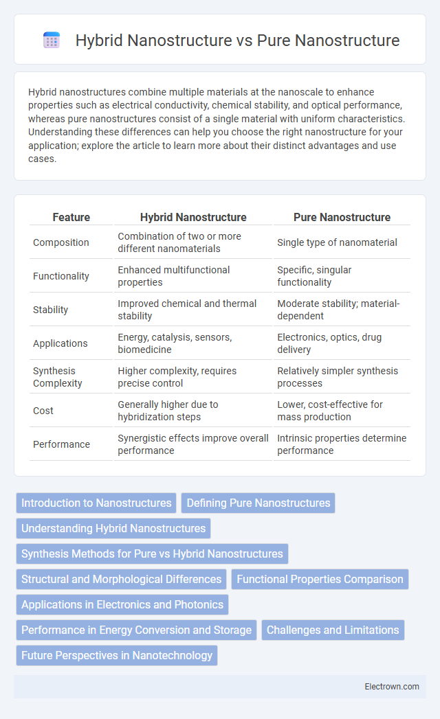
Table of Comparison
| Feature | Hybrid Nanostructure | Pure Nanostructure |
|---|---|---|
| Composition | Combination of two or more different nanomaterials | Single type of nanomaterial |
| Functionality | Enhanced multifunctional properties | Specific, singular functionality |
| Stability | Improved chemical and thermal stability | Moderate stability; material-dependent |
| Applications | Energy, catalysis, sensors, biomedicine | Electronics, optics, drug delivery |
| Synthesis Complexity | Higher complexity, requires precise control | Relatively simpler synthesis processes |
| Cost | Generally higher due to hybridization steps | Lower, cost-effective for mass production |
| Performance | Synergistic effects improve overall performance | Intrinsic properties determine performance |
Introduction to Nanostructures
Nanostructures refer to materials engineered at the nanoscale, exhibiting unique physical and chemical properties due to their size and surface effects. Hybrid nanostructures combine different nanomaterials, such as metals and semiconductors, to enhance functionalities like optical, electronic, and catalytic performance beyond what pure nanostructures offer. Pure nanostructures consist of a single material type, providing well-defined properties but often lacking the synergistic effects seen in hybrid configurations.
Defining Pure Nanostructures
Pure nanostructures consist of a single type of material with uniform composition and structure at the nanoscale, exhibiting distinct physical and chemical properties due to their size and high surface-to-volume ratio. These structures often demonstrate enhanced catalytic activity, optical characteristics, or electronic behavior compared to their bulk counterparts. Their well-defined morphology and composition make pure nanostructures essential for applications in sensors, drug delivery, and nanoelectronics.
Understanding Hybrid Nanostructures
Hybrid nanostructures combine multiple materials at the nanoscale, resulting in enhanced physical, chemical, and electronic properties unattainable by pure nanostructures alone. These engineered composites enable tailored functionalities such as improved catalytic activity, increased stability, and multifunctionality, making them vital for applications in energy storage, sensors, and biomedicine. Understanding hybrid nanostructures allows you to harness their synergistic effects, driving innovation in nanotechnology and materials science.
Synthesis Methods for Pure vs Hybrid Nanostructures
Pure nanostructures are typically synthesized using methods such as sol-gel, chemical vapor deposition (CVD), and hydrothermal synthesis, which allow precise control over particle size and morphology. Hybrid nanostructures involve combining two or more materials via techniques like self-assembly, layer-by-layer deposition, and co-precipitation, enabling enhanced multifunctional properties. Your choice between pure and hybrid nanostructures depends on the complexity of the synthesis process and the targeted application benefits.
Structural and Morphological Differences
Hybrid nanostructures exhibit a combination of multiple materials, resulting in unique interfacial properties and enhanced structural stability compared to pure nanostructures, which consist of a single material phase. Morphologically, hybrid nanostructures often display complex architectures such as core-shell, heterojunctions, or composite assemblies, offering greater surface area and tunable functionalities, while pure nanostructures tend to have uniform shapes like spheres, rods, or sheets with more homogenous surface characteristics. The integration of different components in hybrid systems leads to distinct crystallinity and defect distributions that influence their mechanical and electronic behaviors superiorly to pure counterparts.
Functional Properties Comparison
Hybrid nanostructures exhibit enhanced functional properties compared to pure nanostructures due to synergistic effects between different materials, resulting in improved electrical conductivity, catalytic activity, and mechanical strength. These composites often show superior stability and tunable electronic properties, making them ideal for applications in sensors, energy storage, and catalysis. Pure nanostructures, while simpler, typically possess more uniform but less versatile performance characteristics, limiting their functional adaptability across diverse technologies.
Applications in Electronics and Photonics
Hybrid nanostructures combine materials like metals and semiconductors to enhance electron mobility and light-matter interactions, making them ideal for high-performance electronics and photonic devices such as sensors, lasers, and solar cells. Pure nanostructures, composed of a single material type like graphene or quantum dots, offer exceptional properties including high conductivity and tunable optical responses critical for transistors, LEDs, and photodetectors. Your choice between hybrid and pure nanostructures influences device efficiency, functionality, and integration in advanced electronics and photonics systems.
Performance in Energy Conversion and Storage
Hybrid nanostructures exhibit superior performance in energy conversion and storage due to their synergistic integration of multiple materials, enhancing charge transfer, conductivity, and surface area compared to pure nanostructures. Their tailored interfaces improve catalytic activity and electrochemical stability, leading to higher efficiency and longer cycle life in devices such as batteries, supercapacitors, and solar cells. Your choice of hybrid nanostructures can significantly optimize energy device performance by leveraging these multifunctional properties.
Challenges and Limitations
Hybrid nanostructures face complex challenges including interface defects, material compatibility issues, and synthesis difficulties that can impact their stability and reproducibility compared to pure nanostructures. Pure nanostructures often benefit from more controlled and predictable properties but may lack multifunctionality and enhanced performance achievable in hybrids. Your choice between hybrid and pure nanostructures must consider these trade-offs in scalability, cost, and application-specific stability constraints.
Future Perspectives in Nanotechnology
Hybrid nanostructures combine multiple material properties, enabling enhanced functionality and tunable performance beyond pure nanostructures. Future perspectives in nanotechnology emphasize the development of hybrid systems for applications in energy storage, catalysis, and biomedicine, where synergistic effects improve efficiency and selectivity. Your ability to leverage these advancements will drive innovations in next-generation devices and materials with unprecedented capabilities.
Hybrid Nanostructure vs Pure Nanostructure Infographic