Charge density waves (CDWs) and spin density waves (SDWs) are periodic modulations in the electron density and spin orientation, respectively, which emerge in low-dimensional materials driven by electron-electron interactions or Fermi surface nesting. Understanding the differences between CDWs and SDWs can enhance your insight into complex quantum states and material properties--explore the detailed mechanisms and implications in the rest of this article.
Table of Comparison
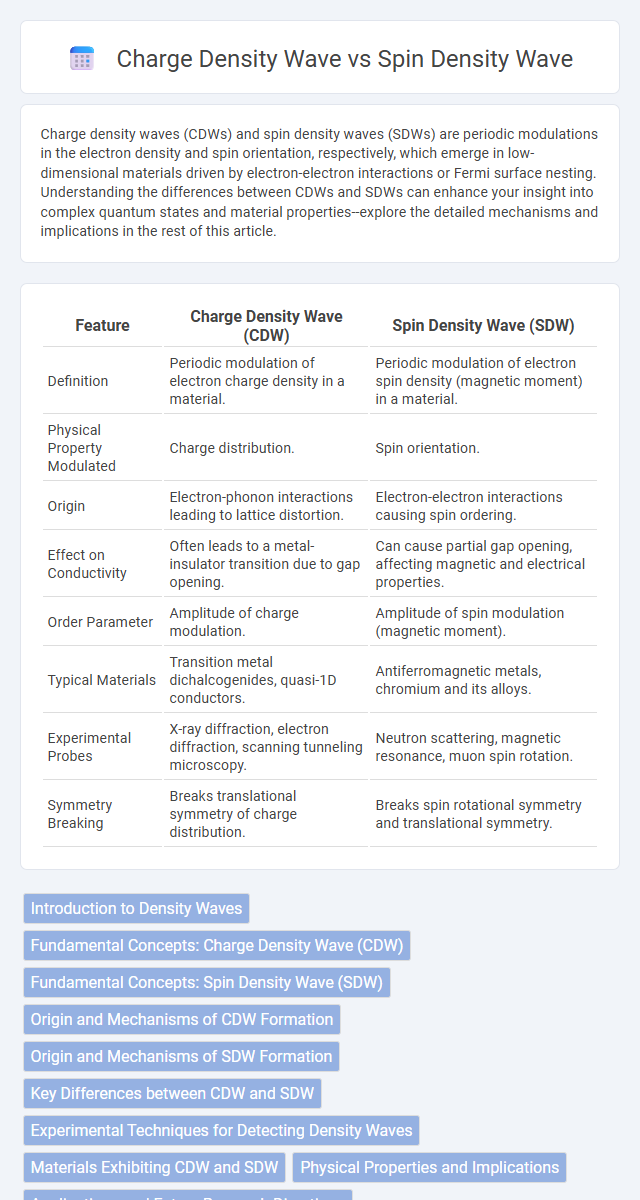
| Feature | Charge Density Wave (CDW) | Spin Density Wave (SDW) |
|---|---|---|
| Definition | Periodic modulation of electron charge density in a material. | Periodic modulation of electron spin density (magnetic moment) in a material. |
| Physical Property Modulated | Charge distribution. | Spin orientation. |
| Origin | Electron-phonon interactions leading to lattice distortion. | Electron-electron interactions causing spin ordering. |
| Effect on Conductivity | Often leads to a metal-insulator transition due to gap opening. | Can cause partial gap opening, affecting magnetic and electrical properties. |
| Order Parameter | Amplitude of charge modulation. | Amplitude of spin modulation (magnetic moment). |
| Typical Materials | Transition metal dichalcogenides, quasi-1D conductors. | Antiferromagnetic metals, chromium and its alloys. |
| Experimental Probes | X-ray diffraction, electron diffraction, scanning tunneling microscopy. | Neutron scattering, magnetic resonance, muon spin rotation. |
| Symmetry Breaking | Breaks translational symmetry of charge distribution. | Breaks spin rotational symmetry and translational symmetry. |
Introduction to Density Waves
Density waves represent periodic modulations in the electronic charge or spin distribution within a material, influencing its electronic properties significantly. Charge density waves (CDWs) arise from the periodic variation of electron density caused by electron-phonon interactions, leading to lattice distortions and reduced electrical conductivity. Spin density waves (SDWs) originate from spin modulations due to electron-electron interactions, often associated with antiferromagnetic ordering and affecting magnetic behavior in low-dimensional conductors.
Fundamental Concepts: Charge Density Wave (CDW)
Charge Density Wave (CDW) is a quantum state in low-dimensional conductors where electron density becomes periodically modulated, creating a wave-like pattern of charge distribution. This phenomenon arises due to electron-phonon interactions leading to a lattice distortion that stabilizes the charge modulation, effectively lowering the system's energy. Understanding CDW is crucial for exploring electrical conductivity and phase transitions in materials, distinguishing it from Spin Density Wave (SDW), which involves periodic modulation of electron spin rather than charge.
Fundamental Concepts: Spin Density Wave (SDW)
Spin Density Wave (SDW) is a quantum ground state characterized by a periodic modulation of electron spin density in a crystalline solid, often driven by electron-electron interactions and Fermi surface nesting. Unlike Charge Density Wave (CDW), which modulates the electronic charge distribution, SDW involves a spatially varying spin polarization that leads to antiferromagnetic order. Materials exhibiting SDW, such as chromium and certain organic conductors, show unique magnetic and transport properties influenced by this spin modulation.
Origin and Mechanisms of CDW Formation
Charge density waves (CDWs) originate from the Peierls instability in quasi-one-dimensional metals, where electron-phonon interactions cause a periodic lattice distortion coupled with a modulation of the electron density, lowering the system's energy. The mechanism involves the nesting of the Fermi surface, which leads to a susceptibility peak at a particular wave vector and stabilizes the charge modulation. Unlike spin density waves (SDWs) that are driven primarily by electron-electron interactions resulting in spin modulation, CDWs arise from electron-phonon coupling and lattice dynamics that synchronize charge redistribution with lattice deformations.
Origin and Mechanisms of SDW Formation
Spin density waves (SDWs) originate from the collective electron spin arrangements in low-dimensional metals, primarily driven by Fermi surface nesting and electron-electron interactions that induce periodic modulation of spin density. Unlike charge density waves, which arise from electron-phonon coupling leading to charge modulation, SDWs result from antiferromagnetic correlations and exchange interactions that stabilize a spin-ordered state with a characteristic wave vector. Understanding the mechanisms of SDW formation can help you explore magnetic properties in materials such as chromium and its alloys, where SDWs significantly influence electronic behavior.
Key Differences between CDW and SDW
Charge density waves (CDWs) involve periodic modulations of the electron charge density within a material, while spin density waves (SDWs) correspond to periodic variations in the electron spin density. CDWs are primarily driven by electron-phonon interactions causing lattice distortions, whereas SDWs arise from electron-electron interactions that lead to magnetic ordering. The distinct physical manifestations of CDWs and SDWs affect electrical conductivity and magnetic properties differently, with CDWs generally leading to charge ordering and SDWs to spin ordering.
Experimental Techniques for Detecting Density Waves
X-ray diffraction and scanning tunneling microscopy are key experimental techniques for detecting charge density waves by revealing periodic lattice distortions and electronic modulations. Neutron scattering and nuclear magnetic resonance provide insights into spin density waves through measurements of magnetic order and local magnetic environments. Angle-resolved photoemission spectroscopy can complement these methods by mapping Fermi surface nesting that drives both charge and spin density waves.
Materials Exhibiting CDW and SDW
Charge density waves (CDWs) commonly occur in low-dimensional materials such as transition metal dichalcogenides (e.g., 1T-TaS2, 2H-NbSe2) and quasi-one-dimensional compounds like K0.3MoO3, where lattice distortions couple with electron density modulations. Spin density waves (SDWs) are primarily observed in antiferromagnetic metals and alloys such as chromium (Cr) and its alloys (Cr-V, Cr-Mn), as well as in some organic conductors and iron-based superconductors, driven by nesting of the Fermi surface leading to spin modulation. Both phenomena reflect correlated electron behaviors, but CDWs involve charge modulation linked to lattice, while SDWs are characterized by spin modulation without necessarily involving lattice distortions.
Physical Properties and Implications
Charge density waves (CDWs) manifest as periodic modulations in electron density coupled with lattice distortions, leading to metal-to-insulator transitions and altering electronic transport properties. Spin density waves (SDWs) involve spatially varying spin polarization without charge modulation, often inducing antiferromagnetic order and impacting magnetic susceptibility and electron scattering. Both phenomena significantly influence low-temperature phases in quasi-one-dimensional conductors, affecting their electronic, magnetic, and structural behaviors.
Applications and Future Research Directions
Charge density waves (CDWs) exhibit potential in nanoelectronics and memory devices due to their tunable electronic properties, while spin density waves (SDWs) offer promise in spintronic applications leveraging their magnetic order. Future research aims to enhance control over phase transitions in CDWs for low-power devices and explore SDW manipulation for quantum computing technologies. Advancements in ultrafast spectroscopies and materials engineering are crucial for unraveling the dynamic behavior and stability of these density waves in novel quantum materials.
Charge density wave vs Spin density wave Infographic