2D semiconductors and 2D metals differ primarily in their electronic properties, with 2D semiconductors exhibiting a tunable bandgap suitable for transistors and optoelectronic devices, while 2D metals provide high electrical conductivity and metallic behavior ideal for interconnects and plasmonic applications. Understanding these distinctions helps you select the right material for advanced nanoelectronics and flexible device engineering; explore the rest of the article to dive deeper into their unique characteristics and applications.
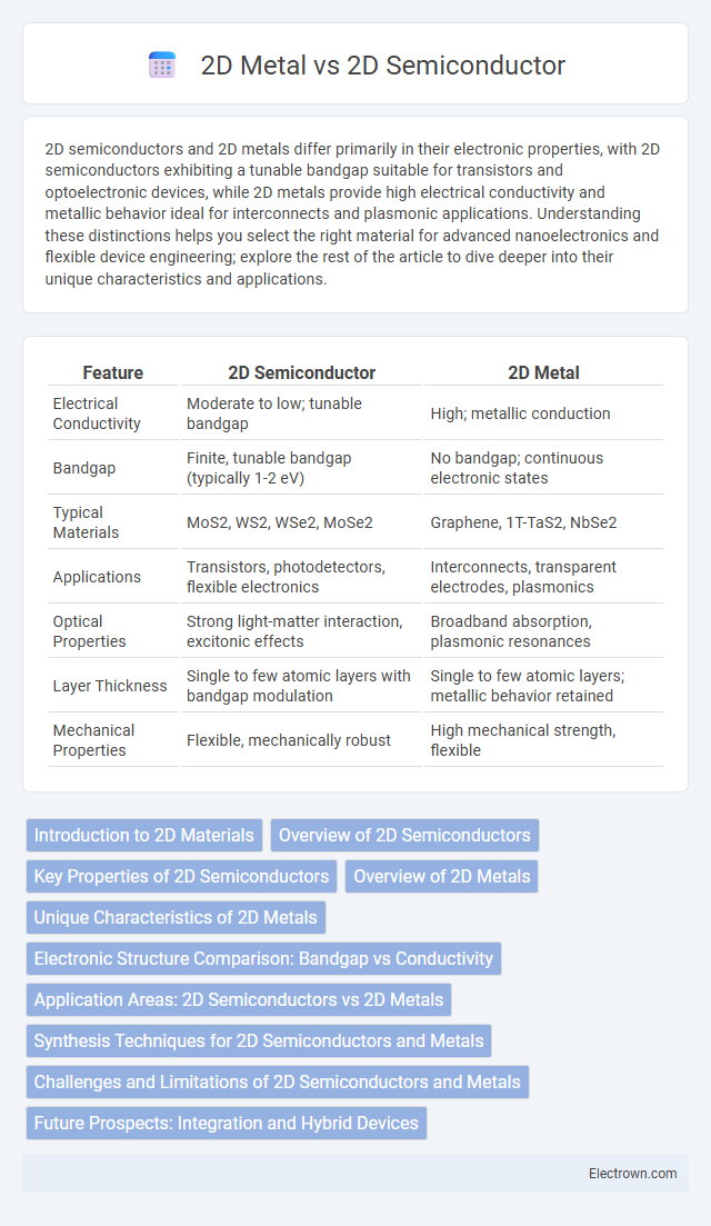
Table of Comparison
| Feature | 2D Semiconductor | 2D Metal |
|---|---|---|
| Electrical Conductivity | Moderate to low; tunable bandgap | High; metallic conduction |
| Bandgap | Finite, tunable bandgap (typically 1-2 eV) | No bandgap; continuous electronic states |
| Typical Materials | MoS2, WS2, WSe2, MoSe2 | Graphene, 1T-TaS2, NbSe2 |
| Applications | Transistors, photodetectors, flexible electronics | Interconnects, transparent electrodes, plasmonics |
| Optical Properties | Strong light-matter interaction, excitonic effects | Broadband absorption, plasmonic resonances |
| Layer Thickness | Single to few atomic layers with bandgap modulation | Single to few atomic layers; metallic behavior retained |
| Mechanical Properties | Flexible, mechanically robust | High mechanical strength, flexible |
Introduction to 2D Materials
2D semiconductors like transition metal dichalcogenides (TMDs) exhibit a tunable bandgap essential for electronic and optoelectronic applications, enabling efficient charge carrier control. In contrast, 2D metals such as graphene offer exceptional electrical conductivity and mechanical strength but lack an inherent bandgap, limiting their use in transistor switching. These unique properties arise from the atomic-scale thickness and crystalline structure of 2D materials, which significantly influence their electronic, optical, and mechanical behavior.
Overview of 2D Semiconductors
2D semiconductors, such as transition metal dichalcogenides (TMDs), exhibit a direct bandgap that enables efficient light absorption and emission, making them ideal for optoelectronic applications. Unlike 2D metals, which have free electrons and high conductivity, 2D semiconductors possess tunable electronic properties that can be controlled through thickness, doping, or strain, offering versatility for transistors, sensors, and photodetectors. Your choice of 2D semiconductor materials impacts device performance by balancing conductivity and bandgap characteristics essential for next-generation electronics.
Key Properties of 2D Semiconductors
2D semiconductors exhibit a tunable bandgap, high carrier mobility, and strong light-matter interaction, which distinguish them from 2D metals characterized by zero bandgap and high electrical conductivity. Materials like transition metal dichalcogenides (e.g., MoS2, WS2) demonstrate unique electronic properties such as direct bandgap in monolayer form, enabling applications in nanoscale transistors and optoelectronic devices. Their atomic-scale thickness and flexibility contribute to enhanced electrostatic control and reduced short-channel effects compared to traditional bulk semiconductors.
Overview of 2D Metals
2D metals consist of atomically thin metallic layers exhibiting high electrical conductivity and unique surface plasmonic properties, making them ideal for nanoelectronics and flexible devices. Unlike 2D semiconductors, which have a bandgap enabling electron modulation, 2D metals lack a bandgap, resulting in metallic behavior with minimal resistance. Prominent examples include monolayer transition metal dichalcogenides in their metallic phases and ultrathin noble metal films, which demonstrate exceptional mechanical flexibility and chemical stability.
Unique Characteristics of 2D Metals
2D metals exhibit high electrical conductivity and exceptional mechanical flexibility due to their atomically thin layers and unique electron transport properties. Their ability to maintain metallic behavior at the atomic scale contrasts with 2D semiconductors, which possess tunable bandgaps essential for electronic and optoelectronic applications. Understanding these unique characteristics helps you leverage 2D metals for applications requiring efficient charge transport and robust mechanical performance.
Electronic Structure Comparison: Bandgap vs Conductivity
2D semiconductors exhibit a distinct electronic structure characterized by a finite bandgap, enabling precise control over electron flow and switching capabilities essential for transistor applications. In contrast, 2D metals possess overlapping conduction and valence bands, resulting in high electrical conductivity and negligible bandgap, which supports efficient charge transport but limits their use in digital logic devices. Understanding these fundamental differences in bandgap and conductivity allows you to select the appropriate material for applications ranging from low-power electronics to transparent conductors.
Application Areas: 2D Semiconductors vs 2D Metals
2D semiconductors are widely used in electronics, optoelectronics, and photodetectors due to their distinct bandgap and excellent charge carrier mobility, making them ideal for transistors, sensors, and flexible devices. In contrast, 2D metals are primarily applied in catalysis, energy storage, and plasmonics because of their high electrical conductivity and catalytic activity. Your choice between 2D semiconductor and 2D metal materials depends on whether your application requires electronic switching capabilities or enhanced conductivity and catalytic performance.
Synthesis Techniques for 2D Semiconductors and Metals
Synthesis techniques for 2D semiconductors, such as transition metal dichalcogenides (TMDs), often involve chemical vapor deposition (CVD) and molecular beam epitaxy (MBE) to achieve precise layer control and high crystallinity. In contrast, 2D metals like graphene or 2D metallic phases typically utilize mechanical exfoliation, CVD, and liquid-phase exfoliation methods, emphasizing scalability and conductivity optimization. Understanding these synthesis approaches enables you to tailor material properties for applications in electronics and optoelectronics.
Challenges and Limitations of 2D Semiconductors and Metals
2D semiconductors face challenges including limited carrier mobility, environmental sensitivity, and difficulty in achieving stable doping, which restricts their performance in electronic devices. On the other hand, 2D metals often suffer from oxidation and phase stability issues, hindering their integration into practical applications. Both materials also grapple with scalability and uniformity problems during synthesis, impacting their commercial viability.
Future Prospects: Integration and Hybrid Devices
2D semiconductors like transition metal dichalcogenides (TMDs) offer tunable bandgaps essential for next-generation transistors and optoelectronic devices, while 2D metals such as graphene provide ultra-high conductivity and flexibility. The future of electronics lies in integrating these materials to create hybrid devices that leverage the complementary properties of both, enabling innovations in flexible displays, sensors, and quantum computing components. Your ability to capitalize on these hybrid structures can drive advancements in performance, energy efficiency, and miniaturization in future technological applications.
2D Semiconductor vs 2D Metal Infographic