In-plane transport refers to the movement of charge carriers or heat within the layers of a material, typically exhibiting higher conductivity due to strong covalent bonding. Out-of-plane transport occurs perpendicular to these layers and generally shows lower conductivity because of weaker van der Waals forces; understanding these differences can significantly impact the design of advanced electronic devices and materials. Explore more to see how Your choice of transport direction influences performance.
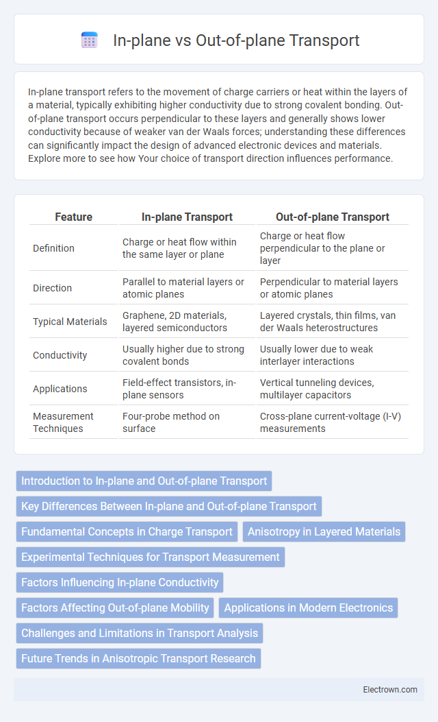
Table of Comparison
| Feature | In-plane Transport | Out-of-plane Transport |
|---|---|---|
| Definition | Charge or heat flow within the same layer or plane | Charge or heat flow perpendicular to the plane or layer |
| Direction | Parallel to material layers or atomic planes | Perpendicular to material layers or atomic planes |
| Typical Materials | Graphene, 2D materials, layered semiconductors | Layered crystals, thin films, van der Waals heterostructures |
| Conductivity | Usually higher due to strong covalent bonds | Usually lower due to weak interlayer interactions |
| Applications | Field-effect transistors, in-plane sensors | Vertical tunneling devices, multilayer capacitors |
| Measurement Techniques | Four-probe method on surface | Cross-plane current-voltage (I-V) measurements |
Introduction to In-plane and Out-of-plane Transport
In-plane transport refers to the movement of charge carriers or energy along the layers or planes of a material, commonly observed in two-dimensional materials such as graphene and transition metal dichalcogenides. Out-of-plane transport involves charge or energy transfer perpendicular to these layers, often characterized by weaker interlayer coupling and lower conductivity compared to in-plane directions. These anisotropic transport properties critically influence the performance of electronic devices, affecting conductivity, mobility, and thermal management in layered nanomaterials.
Key Differences Between In-plane and Out-of-plane Transport
In-plane transport refers to the movement of charge carriers or heat along the same plane, typically within layers of a material, while out-of-plane transport occurs perpendicular to that plane, across layers. Your understanding of key differences lies in anisotropy: in-plane transport usually exhibits higher mobility or conductivity due to stronger bonding and fewer scattering events, whereas out-of-plane transport is often limited by weak interlayer coupling and higher resistance. These distinctions are critical in materials like layered semiconductors and 2D crystals, where electrical and thermal properties vary significantly between these two transport directions.
Fundamental Concepts in Charge Transport
In-plane transport refers to charge movement parallel to the layers of anisotropic materials, while out-of-plane transport occurs perpendicular to these layers, critically influencing electronic device performance. Charge carrier mobility and anisotropic conductivity are fundamental parameters distinguishing these transport modes, dictating efficiency in applications like organic semiconductors and layered transition metal dichalcogenides. Your understanding of these mechanisms is essential for optimizing materials in photovoltaics, transistors, and flexible electronics.
Anisotropy in Layered Materials
Anisotropy in layered materials significantly affects electrical and thermal transport, with in-plane transport exhibiting high conductivity due to strong covalent bonding within layers. Out-of-plane transport is typically limited by weaker van der Waals forces between layers, resulting in reduced carrier mobility and increased resistance. Understanding this directional dependence is crucial for optimizing your device performance in applications such as thermoelectrics and nanoelectronics.
Experimental Techniques for Transport Measurement
Experimental techniques for measuring in-plane and out-of-plane transport include four-point probe methods, Hall effect measurements, and angle-resolved photoemission spectroscopy (ARPES). In-plane transport is typically assessed using van der Pauw or four-probe setups on thin films to minimize contact resistance and maximize accuracy. Out-of-plane transport measurements often require vertical device structures or tunneling spectroscopy to capture charge carrier dynamics across layered materials, enabling precise analysis of anisotropic conductivity essential for optimizing Your electronic and thermoelectric device performance.
Factors Influencing In-plane Conductivity
In-plane conductivity is primarily influenced by the crystal structure, degree of anisotropy, and carrier concentration within the material. Strong covalent bonding and closely packed atomic planes facilitate efficient charge transport along the plane, enhancing electrical conductivity. Your ability to optimize these factors, such as doping levels and lattice orientation, directly impacts the performance of in-plane transport in electronic devices.
Factors Affecting Out-of-plane Mobility
Out-of-plane mobility in layered materials is influenced by interlayer coupling strength, crystal defects, and phonon scattering, which hinder charge carrier movement perpendicular to the layers. The presence of van der Waals gaps and weak interlayer interactions significantly reduce conductivity compared to in-plane transport. Your device performance can be optimized by engineering layer stacking and minimizing impurities to enhance out-of-plane charge transport efficiency.
Applications in Modern Electronics
In-plane transport facilitates high-speed electron flow within the same layer of 2D materials, crucial for efficient operation in flexible electronics and ultra-thin transistors. Out-of-plane transport governs electron movement perpendicular to layers, enabling vertical device architectures like tunnel diodes and memory cells in advanced semiconductor technologies. Understanding these transport mechanisms enhances Your ability to optimize device performance for applications such as sensors, energy storage, and next-generation integrated circuits.
Challenges and Limitations in Transport Analysis
In-plane transport analysis faces challenges such as anisotropic material properties and electron scattering at grain boundaries, which complicate accurate modeling of charge carrier mobility. Out-of-plane transport is limited by weak interlayer coupling and increased resistance due to van der Waals gaps, making it difficult to achieve consistent conductivity across stratified materials. Both transport modes require advanced characterization techniques and multiscale simulation approaches to overcome limitations in spatial resolution and heterogeneity of layered structures.
Future Trends in Anisotropic Transport Research
Future trends in anisotropic transport research emphasize the enhancement of in-plane and out-of-plane charge carrier mobility through advanced material engineering, such as 2D van der Waals heterostructures and layered organic semiconductors. Emerging techniques in nanoscale characterization and computational modeling will enable precise tuning of anisotropic conduction pathways, optimizing device performance for applications in flexible electronics and energy storage. Your understanding of these developments is crucial for leveraging anisotropic materials in next-generation nanoelectronic and optoelectronic systems.
In-plane vs Out-of-plane transport Infographic