Ion gel gating offers superior capacitance and enables low-voltage operation compared to conventional dielectric gating, enhancing the performance of flexible and wearable electronics. Discover how your choice between ion gel and traditional dielectrics can impact device efficiency and scalability by reading the full article.
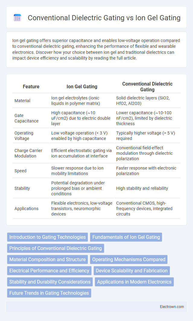
Table of Comparison
| Feature | Ion Gel Gating | Conventional Dielectric Gating |
|---|---|---|
| Material | Ion gel electrolytes (ionic liquids in polymer matrix) | Solid dielectric layers (SiO2, HfO2, Al2O3) |
| Gate Capacitance | High capacitance (~10 uF/cm2) due to electric double layer | Lower capacitance (~10-100 nF/cm2), limited by dielectric thickness |
| Operating Voltage | Low voltage operation (< 3 V) enabled by high capacitance | Typically higher voltage (> 5 V) required |
| Charge Carrier Modulation | Efficient electrostatic gating via ion accumulation at interface | Conventional field-effect modulation through dielectric polarization |
| Speed | Slower response due to ion mobility limitations | Faster response with electronic polarization |
| Stability | Potential degradation under prolonged bias or ambient conditions | High stability and reliability |
| Applications | Flexible electronics, low-voltage transistors, neuromorphic devices | Conventional CMOS, high-frequency devices, integrated circuits |
Introduction to Gating Technologies
Ion gel gating utilizes a polymer electrolyte to form an electric double layer with extremely high capacitance, enabling efficient modulation of carrier density in semiconductors at low voltages. Conventional dielectric gating relies on solid insulating materials like silicon dioxide or hafnium oxide to control the channel conductivity through an applied electric field, but typically requires higher operating voltages and offers lower capacitance. Your choice between these gating technologies impacts device performance, power consumption, and scalability for applications in flexible electronics and low-power transistors.
Fundamentals of Ion Gel Gating
Ion gel gating utilizes an electrolyte-based material that forms an electric double layer with exceptionally high capacitance at the semiconductor interface, enabling efficient charge carrier accumulation at low operating voltages. This mechanism differs from conventional dielectric gating, which relies on solid insulating oxides with fixed dielectric constants and limited capacitance, thereby requiring higher voltages for comparable charge modulation. The fundamental advantage of ion gel gating lies in its ion migration and accumulation properties, facilitating enhanced electrostatic control and tunable charge density in next-generation electronic devices.
Principles of Conventional Dielectric Gating
Conventional dielectric gating relies on an insulating layer, typically silicon dioxide or high-k materials, to separate the gate electrode from the semiconductor channel, enabling charge modulation through an electric field without direct charge transfer. The dielectric material's capacitance directly influences the device's threshold voltage, subthreshold slope, and overall switching speed by controlling the electric field strength across the channel. This gating method ensures stable operation in field-effect transistors (FETs) but may face limitations in achieving high carrier densities and low voltage operation compared to ion gel gating.
Material Composition and Structure
Ion gel gating utilizes ion-conductive polymer matrices imbued with mobile ions, forming an electric double layer at the interface that enables high capacitance and low voltage operation. Conventional dielectric gating relies on insulating materials like SiO2 or HfO2 with fixed dielectric constants and layered crystalline or amorphous structures to control channel conductivity through the field effect. Your choice between these gating methods depends on the desired material flexibility, capacitance density, and operating voltage characteristics for specific electronic applications.
Operating Mechanisms Compared
Ion gel gating operates through the formation of an electric double layer (EDL) at the interface between the ion gel and the semiconductor, enabling extremely high capacitance and facilitating efficient charge carrier accumulation at low voltages. Conventional dielectric gating relies on a solid dielectric layer to induce charge carriers via an electric field across the material, typically showing lower capacitance and requiring higher operating voltages. The key distinction lies in ion gel gating's utilization of mobile ions to achieve ultra-thin effective dielectric thickness, resulting in enhanced device performance and reduced power consumption compared to traditional dielectric gating.
Electrical Performance and Efficiency
Ion gel gating offers superior electrical performance compared to conventional dielectric gating by enabling higher capacitance and lower operating voltages, which enhances device efficiency. The ionic conductivity and large electrochemical window of ion gels result in faster switching speeds and reduced power consumption in transistors. Conventional dielectrics typically suffer from lower capacitance density and higher leakage currents, limiting their efficiency and performance in high-frequency applications.
Device Scalability and Fabrication
Ion gel gating offers superior device scalability compared to conventional dielectric gating due to its ultra-thin, flexible structure that enables high capacitance at low operating voltages, which reduces power consumption and allows for miniaturized device designs. Fabrication of ion gel-gated devices is often simpler and compatible with low-temperature, solution-based processes, facilitating integration with flexible substrates and large-area electronics. Your choice of gating method can significantly impact the overall device performance and manufacturing cost efficiency, especially in scalable applications.
Stability and Durability Considerations
Ion gel gating offers superior stability and durability compared to conventional dielectric gating by providing enhanced mechanical flexibility and resistance to environmental degradation. The ion gel's robust electrochemical properties maintain consistent performance under prolonged electrical stress and temperature variations. Your devices benefit from reduced leakage currents and improved interface stability, ensuring longer operational lifetimes and reliable functionality.
Applications in Modern Electronics
Ion gel gating enables high capacitance and low voltage operation, making it ideal for flexible and wearable electronics that require efficient charge modulation. Conventional dielectric gating remains essential in traditional semiconductor devices like transistors and integrated circuits, offering stability and scalability for mass production. Your choice between these gating methods depends on the device's performance needs and application context in modern electronics development.
Future Trends in Gating Technologies
Ion gel gating offers enhanced electrostatic control and flexibility for next-generation flexible electronics, enabling low-voltage operation and improved device scalability compared to conventional dielectric gating. Advances in ion gel materials with high ionic conductivity and chemical stability are driving the integration of ion gels in wearable sensors and neuromorphic devices. Future trends indicate a shift toward hybrid gating architectures combining ion gels with traditional dielectrics to optimize performance, energy efficiency, and device longevity in emerging semiconductor technologies.
Ion Gel Gating vs Conventional Dielectric Gating Infographic