CMOS technology has been the foundation of digital circuits for decades, but FinFET architecture offers superior scalability, reduced leakage current, and enhanced performance at smaller nanometer scales. Explore the full comparison to understand how these advancements could impact Your next semiconductor design choices.
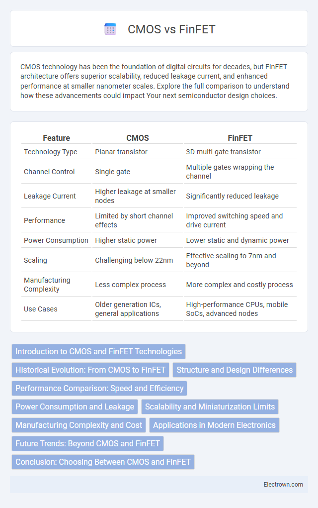
Table of Comparison
| Feature | CMOS | FinFET |
|---|---|---|
| Technology Type | Planar transistor | 3D multi-gate transistor |
| Channel Control | Single gate | Multiple gates wrapping the channel |
| Leakage Current | Higher leakage at smaller nodes | Significantly reduced leakage |
| Performance | Limited by short channel effects | Improved switching speed and drive current |
| Power Consumption | Higher static power | Lower static and dynamic power |
| Scaling | Challenging below 22nm | Effective scaling to 7nm and beyond |
| Manufacturing Complexity | Less complex process | More complex and costly process |
| Use Cases | Older generation ICs, general applications | High-performance CPUs, mobile SoCs, advanced nodes |
Introduction to CMOS and FinFET Technologies
CMOS technology has been the foundation of semiconductor devices, utilizing planar transistors to achieve low power consumption and high integration density. FinFET technology represents an evolution, employing a 3D fin-shaped structure that enhances control over the channel, reducing leakage currents and improving performance at smaller nodes. Your choice between CMOS and FinFET impacts device efficiency, scalability, and suitability for advanced applications in modern electronics.
Historical Evolution: From CMOS to FinFET
The historical evolution from CMOS to FinFET reflects significant advancements in transistor technology aimed at overcoming scaling challenges and improving device performance. CMOS technology, dominant since the 1960s, faced physical limitations like short-channel effects and leakage currents as device dimensions shrank below 20 nanometers. FinFET architecture, introduced in the early 2010s, offers enhanced electrostatic control and reduced power consumption by using a three-dimensional fin structure, enabling continued transistor scaling and improved performance in modern integrated circuits.
Structure and Design Differences
CMOS technology uses planar transistors with a single gate controlling the channel, while FinFETs feature a three-dimensional fin-shaped channel wrapped by multiple gates, improving electrostatic control. FinFET designs reduce short-channel effects and leakage currents due to their multi-gate architecture, enabling better scalability at smaller nodes. The complex 3D structure of FinFETs requires advanced fabrication techniques compared to the simpler planar layout of CMOS transistors.
Performance Comparison: Speed and Efficiency
FinFET technology significantly outperforms traditional CMOS in speed due to its three-dimensional structure, which reduces short-channel effects and leakage current, enabling higher drive currents and faster switching speeds. FinFETs also offer improved power efficiency by lowering off-state leakage and reducing dynamic power consumption compared to planar CMOS transistors. This results in enhanced overall performance for integrated circuits, particularly in high-density, low-power applications such as mobile processors and advanced computing systems.
Power Consumption and Leakage
FinFET technology significantly reduces power consumption and leakage current compared to traditional CMOS due to its 3D gate structure that provides better electrostatic control over the channel. This improved control minimizes short-channel effects and subthreshold leakage, enabling lower voltage operation and enhanced energy efficiency. As a result, FinFET transistors are preferred in advanced low-power integrated circuits and high-performance applications.
Scalability and Miniaturization Limits
Finite scaling challenges of CMOS technology become critical below 10nm, where short-channel effects, leakage currents, and power dissipation hinder further miniaturization. FinFET architecture, with its 3D multi-gate design, offers superior electrostatic control and reduced leakage, enabling gate lengths as small as 5nm while maintaining performance and power efficiency. This scalability advantage positions FinFET as the preferred transistor technology for advanced nodes beyond 7nm, addressing the miniaturization limits faced by traditional planar CMOS.
Manufacturing Complexity and Cost
FinFET devices exhibit higher manufacturing complexity compared to traditional CMOS due to their three-dimensional structure requiring advanced lithography and precise etching techniques. The increased fabrication challenges lead to higher production costs for FinFET technology, especially at smaller technology nodes below 10 nm. However, despite the elevated expense, FinFETs offer improved performance and energy efficiency that can justify the investment for cutting-edge semiconductor applications.
Applications in Modern Electronics
CMOS technology remains prevalent in low-power and high-density applications such as microcontrollers and sensors, benefiting from mature fabrication processes. FinFET devices dominate high-performance computing and mobile processors due to their superior control over short-channel effects and reduced leakage currents at nanoscale dimensions. The shift towards FinFET-based designs fosters advancements in AI chips and 5G technology, driving enhanced speed and energy efficiency in modern electronics.
Future Trends: Beyond CMOS and FinFET
Future trends in semiconductor technology explore Beyond CMOS and FinFET approaches such as Tunnel FETs, spintronics, and 2D materials like graphene and transition metal dichalcogenides for enhanced performance and energy efficiency. Research focuses on overcoming FinFET scaling limitations by developing novel device architectures and quantum computing components. These advancements aim to sustain Moore's Law and enable ultra-low-power, high-speed circuits in next-generation electronics.
Conclusion: Choosing Between CMOS and FinFET
Choosing between CMOS and FinFET hinges on your specific design goals, power efficiency, and scaling requirements. CMOS technology offers cost-effectiveness and simplicity for lower-performance applications, while FinFET provides superior control over short-channel effects and enables higher transistor density in advanced nodes. Your decision should balance the trade-offs between manufacturing complexity and performance gains to meet the demands of modern integrated circuits.
CMOS vs FinFET Infographic