Ion implantation offers precise doping control by embedding ions directly into the semiconductor lattice, enhancing device performance without altering the substrate's bulk properties. Molecular beam epitaxy, on the other hand, enables the growth of ultra-thin crystalline layers with atomic-scale precision, ideal for fabricating high-quality semiconductor heterostructures; explore the full article to understand which technique best suits your semiconductor fabrication needs.
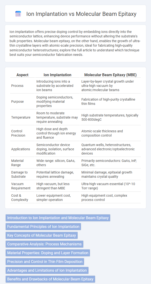
Table of Comparison
| Aspect | Ion Implantation | Molecular Beam Epitaxy (MBE) |
|---|---|---|
| Process | Introducing ions into a substrate by accelerated ion beams | Layer-by-layer crystal growth under ultra-high vacuum by atomic/molecular beams |
| Purpose | Doping semiconductors, modifying material properties | Fabrication of high-purity crystalline thin films |
| Temperature | Room to moderate temperature, substrate may require annealing | High substrate temperatures, typically 500-800degC |
| Control Precision | High dose and depth control through ion energy and fluence | Atomic-scale thickness and composition control |
| Applications | Semiconductor device doping, isolation, surface modification | Quantum wells, heterostructures, advanced electronic/optoelectronic devices |
| Material Range | Wide range: silicon, GaAs, others | Primarily semiconductors: GaAs, InP, SiGe, etc. |
| Damage to Substrate | Potential lattice damage, requires annealing | Minimal damage, epitaxial growth maintains crystal quality |
| Vacuum Requirement | High vacuum, but less stringent than MBE | Ultra-high vacuum essential (10^-10 Torr range) |
| Cost & Complexity | Lower equipment cost, simpler operation | High equipment cost, complex process control |
Introduction to Ion Implantation and Molecular Beam Epitaxy
Ion implantation is a precise semiconductor fabrication technique that introduces dopant ions into a substrate, enabling controlled modification of electrical properties. Molecular Beam Epitaxy (MBE) allows for the growth of ultra-thin crystalline layers with atomic-scale precision, essential for producing high-quality semiconductor devices. Understanding these methods helps optimize your device performance through tailored material engineering.
Fundamental Principles of Ion Implantation
Ion implantation involves accelerating ions to high energies and directing them into a semiconductor substrate to alter its physical, chemical, or electrical properties by creating doped regions with precise depth and concentration profiles. This process enables atomic-scale control of impurity distribution, crucial for fabricating integrated circuits and modifying material characteristics without altering the substrate's crystallinity. Unlike Molecular Beam Epitaxy, which deposits atomic layers to grow thin films, ion implantation modifies existing materials through energetic ion bombardment, impacting lattice structures and electrical behavior.
Key Concepts of Molecular Beam Epitaxy
Molecular Beam Epitaxy (MBE) is a precise thin-film deposition technique that constructs crystalline layers by directing atomic or molecular beams onto a heated substrate under ultra-high vacuum. This method enables atomic-level control of layer thickness, composition, and doping, essential for fabricating semiconductor devices with high purity and abrupt interfaces. Your ability to tailor complex heterostructures makes MBE indispensable in advanced research and commercial applications like quantum wells and high-electron-mobility transistors.
Comparative Analysis: Process Mechanisms
Ion implantation introduces high-energy ions into a semiconductor substrate, creating controlled dopant profiles through physical penetration and collision cascades, while Molecular Beam Epitaxy (MBE) deposits atomic or molecular beams layer-by-layer under ultra-high vacuum conditions, enabling precise control of crystal growth and composition. Ion implantation disrupts the lattice structure, necessitating post-implantation annealing to restore crystallinity, whereas MBE inherently produces epitaxial layers with atomic-level uniformity and minimal defects. The implantation depth and concentration in ion implantation are governed by ion energy and dose, whereas MBE allows atomic-scale engineering of interfaces and heterostructures through flux rates and shutter timing.
Material Properties: Doping and Layer Formation
Ion implantation introduces precise dopant atoms into semiconductors by accelerating ions into the substrate, enabling controlled doping concentrations and profiles critical for device performance. Molecular beam epitaxy (MBE) allows atomic-layer-by-layer growth of high-purity crystalline films with exceptional control over composition and thickness, forming abrupt interfaces and complex multilayers. Your choice between ion implantation and MBE impacts material properties such as dopant distribution uniformity and layer quality, essential for optimizing electronic and optoelectronic device fabrication.
Precision and Control in Thin Film Deposition
Ion implantation offers exceptional precision in doping by enabling controlled ion energy and dose, precisely adjusting the depth and concentration of dopants within a substrate. Molecular beam epitaxy (MBE) provides atomic-level control over thin film growth, allowing for the fabrication of highly uniform and defect-free layers with precise thickness and composition. MBE excels in producing complex heterostructures with sharp interfaces, while ion implantation is typically used for localized modification of material properties in semiconductor device fabrication.
Advantages and Limitations of Ion Implantation
Ion implantation offers precise control over doping concentration and depth, enabling high repeatability for semiconductor device fabrication. However, this technique can cause crystal damage and requires subsequent annealing to repair the lattice structure, which may affect material quality. Your choice of ion implantation must balance these advantages with limitations compared to molecular beam epitaxy, which allows atomically precise thin-film growth but lacks the same doping flexibility.
Benefits and Drawbacks of Molecular Beam Epitaxy
Molecular Beam Epitaxy (MBE) enables precise atomic layer control, making it ideal for creating high-quality semiconductor heterostructures with excellent interface sharpness and purity. The process operates under ultra-high vacuum conditions, reducing contamination and allowing for in-situ monitoring, which enhances material characterization and reproducibility. However, MBE is costly, relatively slow, and limited in throughput compared to other methods like ion implantation, restricting its use mainly to research and specialized device fabrication.
Applications in Semiconductor Device Fabrication
Ion implantation enables precise doping of semiconductors by embedding ions at controlled depths, making it ideal for creating p-n junctions and modifying electrical properties in integrated circuits. Molecular beam epitaxy (MBE) facilitates atomic-level deposition of ultra-thin, high-purity semiconductor layers, critical for fabricating advanced devices like quantum wells, superlattices, and high-electron-mobility transistors. Your choice between these techniques depends on whether you need controlled doping profiles or epitaxial layer growth for cutting-edge semiconductor device fabrication.
Future Trends in Ion Implantation and Molecular Beam Epitaxy
Emerging advancements in ion implantation focus on ultra-precise dopant placement and 3D device architectures, enabling next-generation semiconductor performance. Molecular beam epitaxy (MBE) continues to evolve with atomic layer control and integration of novel materials like 2D semiconductors for quantum computing and optoelectronics. Your semiconductor fabrication can benefit from combining ion implantation's scalability with MBE's atomic precision to drive future innovation in device miniaturization and heterostructure engineering.
Ion implantation vs Molecular beam epitaxy Infographic