Phase engineering focuses on controlling the crystalline phase of materials to enhance their electronic, optical, or catalytic properties, while doping engineering involves introducing impurities into a material to modify its electrical conductivity and carrier concentration. Understanding these techniques is crucial for advancing your material design strategies; explore the article to learn how each approach can optimize performance in various applications.
Table of Comparison
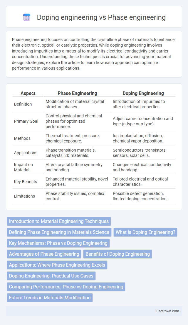
| Aspect | Phase Engineering | Doping Engineering |
|---|---|---|
| Definition | Modification of material crystal structure phases. | Introduction of impurities to alter electrical properties. |
| Primary Goal | Control physical and chemical phases for optimized performance. | Adjust carrier concentration and type (n-type or p-type). |
| Methods | Thermal treatment, pressure, chemical exposure. | Ion implantation, diffusion, chemical vapor deposition. |
| Applications | Phase transition materials, catalysts, 2D materials. | Semiconductors, transistors, sensors, solar cells. |
| Impact on Material | Alters crystal lattice symmetry and bonding. | Changes electrical conductivity and bandgap. |
| Key Benefits | Enhanced material stability, novel properties. | Tailored electrical and optical characteristics. |
| Limitations | Phase stability issues, complex control. | Possible defect generation, limited doping concentration. |
Introduction to Material Engineering Techniques
Phase engineering involves altering the crystal structure of materials to enhance properties like conductivity and stability, while doping engineering focuses on introducing impurities to modify electrical characteristics and carrier concentration. Both techniques are essential in material engineering for tailoring functionality in semiconductors, sensors, and electronic devices. Your choice between phase and doping engineering depends on the desired material performance and application requirements.
Defining Phase Engineering in Materials Science
Phase engineering in materials science involves controlling and manipulating the crystal phases of a material to tailor its physical, chemical, and electronic properties, distinct from doping engineering which introduces impurities to alter conductivity or reactivity. By precisely tuning the phase composition, researchers can optimize properties such as catalytic activity, stability, and mechanical strength without changing the material's elemental makeup. Your ability to harness phase engineering enables the design of advanced materials with targeted functionalities for applications in electronics, energy storage, and catalysis.
What is Doping Engineering?
Doping engineering involves intentionally introducing impurities into a semiconductor to modify its electrical properties and enhance device performance. This process controls carrier concentration and conductivity, enabling precise tuning of materials such as silicon or graphene for applications in transistors, sensors, and photovoltaics. Unlike phase engineering, which alters the material's crystal structure, doping engineering focuses specifically on impurity addition to achieve desired electronic characteristics.
Key Mechanisms: Phase vs Doping Engineering
Phase engineering involves altering the crystal structure or phase of a material to modify its electronic, optical, and mechanical properties, such as converting MoS2 from a semiconducting 2H phase to a metallic 1T phase, enhancing conductivity. Doping engineering introduces impurity atoms into a host material, like adding phosphorus or boron to silicon, which changes carrier concentration and type to tailor electrical characteristics. Your material's performance can be strategically controlled by choosing phase engineering for structural transformation or doping engineering for carrier manipulation.
Advantages of Phase Engineering
Phase engineering enhances material properties by precisely controlling crystal structures, leading to improved electrical conductivity, thermal stability, and mechanical strength in semiconductors. It allows for tunable bandgaps and phase transitions, optimizing performance for applications such as photovoltaics, catalysis, and electronic devices. Compared to doping engineering, phase engineering introduces fewer defects and maintains intrinsic material integrity, resulting in superior long-term device reliability and efficiency.
Benefits of Doping Engineering
Doping engineering enhances semiconductor performance by precisely introducing impurity atoms, which adjusts electrical conductivity and carrier concentration for tailored device functionality. It enables improved control over the material's electrical properties, boosting efficiency and speed in electronic components like transistors and solar cells. Your devices benefit from increased performance, reduced power consumption, and enhanced reliability through optimized doping strategies.
Applications: Where Phase Engineering Excels
Phase engineering excels in applications such as enhancing the catalytic performance of transition metal dichalcogenides (TMDs) for hydrogen evolution reactions and improving the electronic conductivity in energy storage devices like lithium-ion batteries and supercapacitors. It enables precise control over material phases to tailor optical, mechanical, and thermal properties essential in flexible electronics and photodetectors. Unlike doping engineering that primarily modifies charge carrier density, phase engineering offers superior tunability in phase-dependent functionalities critical for next-generation nanoelectronics and optoelectronics.
Doping Engineering: Practical Use Cases
Doping engineering involves intentionally introducing impurities into semiconductors to alter electrical properties, enabling the creation of p-type or n-type materials essential for transistor function in integrated circuits. Practical use cases include enhancing silicon wafer conductivity in microprocessors, optimizing charge carrier concentration for photovoltaic cells, and improving sensor sensitivity in gas detection devices. This precise control over semiconductor performance is fundamental in developing advanced electronics and energy-efficient components.
Comparing Performance: Phase vs Doping Engineering
Phase engineering significantly enhances electronic properties by altering the crystal lattice structure, resulting in improved carrier mobility and thermal stability in semiconductor materials. In contrast, doping engineering introduces impurity atoms to modulate carrier concentration and tailor electrical conductivity, offering precise control over device characteristics. While phase engineering provides structural and phase-dependent performance boosts, doping engineering excels in fine-tuning electronic behavior, making their combined application essential for optimizing next-generation optoelectronic devices.
Future Trends in Materials Modification
Phase engineering and doping engineering are pivotal strategies in materials modification, with future trends emphasizing atomically precise control to enhance electronic, optical, and mechanical properties. Advanced techniques such as in situ characterization and machine learning-driven synthesis are accelerating the discovery of novel phases and dopant configurations, enabling tailored functionalities for applications in semiconductors, energy storage, and catalysis. Integration of phase and doping modulation at the nanoscale will drive the development of next-generation multifunctional materials with unprecedented performance and adaptability.
Phase engineering vs Doping engineering Infographic