Ballistic conduction occurs when electrons travel through a material without scattering, enabling ultra-fast signal transmission at the nanoscale, whereas quantum confinement restricts electron motion within nanostructures, altering their energy levels and electronic properties. Understanding how these phenomena impact device performance can help you optimize nanotechnology applications--read on to explore their key differences and practical implications.
Table of Comparison
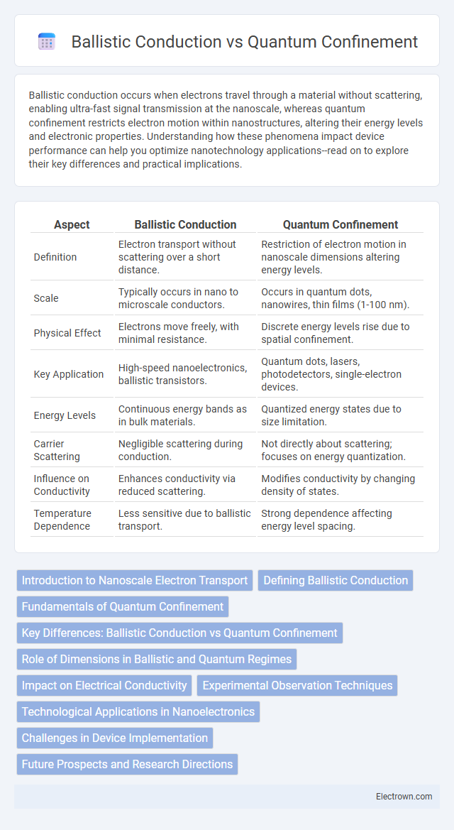
| Aspect | Ballistic Conduction | Quantum Confinement |
|---|---|---|
| Definition | Electron transport without scattering over a short distance. | Restriction of electron motion in nanoscale dimensions altering energy levels. |
| Scale | Typically occurs in nano to microscale conductors. | Occurs in quantum dots, nanowires, thin films (1-100 nm). |
| Physical Effect | Electrons move freely, with minimal resistance. | Discrete energy levels rise due to spatial confinement. |
| Key Application | High-speed nanoelectronics, ballistic transistors. | Quantum dots, lasers, photodetectors, single-electron devices. |
| Energy Levels | Continuous energy bands as in bulk materials. | Quantized energy states due to size limitation. |
| Carrier Scattering | Negligible scattering during conduction. | Not directly about scattering; focuses on energy quantization. |
| Influence on Conductivity | Enhances conductivity via reduced scattering. | Modifies conductivity by changing density of states. |
| Temperature Dependence | Less sensitive due to ballistic transport. | Strong dependence affecting energy level spacing. |
Introduction to Nanoscale Electron Transport
Nanoscale electron transport involves understanding unique phenomena such as ballistic conduction and quantum confinement, critical for designing next-generation electronic devices. Ballistic conduction occurs when electrons travel through a conductor without scattering, maintaining high-speed and low-resistance flow over nanometer distances. Quantum confinement arises when the electron motion is restricted to dimensions comparable to its wavelength, altering electronic properties and enabling precise control of device behavior at the nanoscale.
Defining Ballistic Conduction
Ballistic conduction refers to the transport of electrons through a material without scattering, allowing them to travel freely over nanoscale distances. This phenomenon is critical in nanoscale devices, where electron mean free paths exceed the channel length, enabling ultra-fast and energy-efficient conduction. Your device performance benefits significantly from ballistic conduction by minimizing resistance and heat generation.
Fundamentals of Quantum Confinement
Quantum confinement occurs when electrons are restricted to dimensions comparable to their de Broglie wavelength, altering their energy levels and electronic properties. This phenomenon leads to discrete energy states and quantized charge carrier behavior, significantly impacting semiconductors and nanostructures like quantum wells, wires, and dots. Understanding quantum confinement is essential for designing nanoscale devices with enhanced optical and electrical performance.
Key Differences: Ballistic Conduction vs Quantum Confinement
Ballistic conduction occurs when electrons travel through a material without scattering, maintaining their momentum over nanometer distances, crucial for high-speed nanoscale electronic devices. Quantum confinement arises when electrons are confined to extremely small dimensions, typically in quantum dots or nanowires, leading to discrete energy levels and altered electronic properties. Understanding these key differences helps you optimize materials for applications like quantum computing or ultra-fast transistors.
Role of Dimensions in Ballistic and Quantum Regimes
Dimensions critically influence electron transport in ballistic conduction, where electrons travel without scattering through nanoscale channels typically shorter than the electron mean free path. Quantum confinement arises in even smaller dimensions, such as quantum dots or nanowires, where electron wavefunctions are spatially restricted, leading to discrete energy levels and altered electronic properties. These dimensional effects dictate whether electron behavior is dominated by ballistic transport or quantum confinement phenomena, impacting device performance in nanoelectronics.
Impact on Electrical Conductivity
Ballistic conduction enables electrons to travel through a material without scattering, significantly enhancing electrical conductivity by minimizing resistance at nanoscale dimensions. Quantum confinement modifies the electronic band structure, leading to discrete energy levels that can either increase or decrease conductivity depending on the size and material properties. These phenomena are critical in designing nanoscale devices, as ballistic conduction improves charge transport efficiency, while quantum confinement allows precise tuning of electrical characteristics.
Experimental Observation Techniques
Ballistic conduction is experimentally observed using low-temperature transport measurements in mesoscopic devices, where electron scattering is minimized to detect near-ballistic electron flow. Quantum confinement effects are typically analyzed through scanning tunneling microscopy (STM) and photoluminescence spectroscopy, which reveal discrete energy levels in quantum dots or nanowires. You can rely on electron transport spectroscopy and magneto-transport experiments to differentiate ballistic conduction from quantum confinement phenomena in semiconductor nanostructures.
Technological Applications in Nanoelectronics
Ballistic conduction enables ultra-fast electron transport in nanoscale devices by minimizing scattering, crucial for the development of high-speed transistors and interconnects in nanoelectronics. Quantum confinement alters electronic properties by restricting electron motion within nanoscale dimensions, essential for designing quantum dots and nanoscale sensors with enhanced performance. Both phenomena drive advances in semiconductor technology, enabling devices with improved energy efficiency, speed, and integration density.
Challenges in Device Implementation
Ballistic conduction faces challenges such as maintaining electron coherence over device lengths, requiring materials with minimal impurities and defects to reduce scattering. Quantum confinement demands precise control over nanoscale dimensions to achieve discrete energy levels, often limited by fabrication inconsistencies and variability. Your devices must balance these complexities to optimize performance in nanoelectronic applications.
Future Prospects and Research Directions
Future prospects for ballistic conduction emphasize developing nanoscale materials and devices that exploit near-zero resistance electron transport to enhance circuit speed and energy efficiency. Research directions in quantum confinement focus on manipulating electron wavefunctions within quantum wells, dots, and wires to achieve unprecedented control over electronic and optical properties for quantum computing and advanced sensors. Integrating ballistic conduction phenomena with quantum confinement techniques promises breakthroughs in next-generation transistor architectures and low-power nanoelectronics.
Ballistic Conduction vs Quantum Confinement Infographic