Quantum wells confine charge carriers in one dimension, creating a two-dimensional electron gas with enhanced optical and electronic properties, while quantum wires restrict carriers in two dimensions, resulting in quasi-one-dimensional transport and increased quantum confinement effects. Explore the article to understand how these differences impact your applications in nanotechnology and optoelectronics.
Table of Comparison
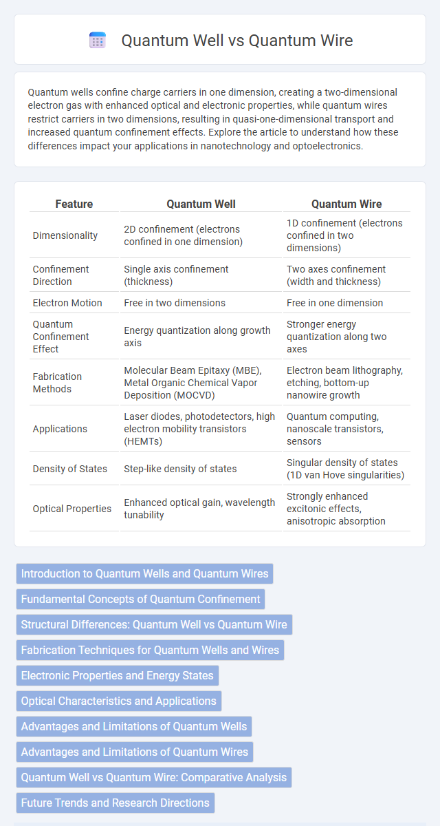
| Feature | Quantum Well | Quantum Wire |
|---|---|---|
| Dimensionality | 2D confinement (electrons confined in one dimension) | 1D confinement (electrons confined in two dimensions) |
| Confinement Direction | Single axis confinement (thickness) | Two axes confinement (width and thickness) |
| Electron Motion | Free in two dimensions | Free in one dimension |
| Quantum Confinement Effect | Energy quantization along growth axis | Stronger energy quantization along two axes |
| Fabrication Methods | Molecular Beam Epitaxy (MBE), Metal Organic Chemical Vapor Deposition (MOCVD) | Electron beam lithography, etching, bottom-up nanowire growth |
| Applications | Laser diodes, photodetectors, high electron mobility transistors (HEMTs) | Quantum computing, nanoscale transistors, sensors |
| Density of States | Step-like density of states | Singular density of states (1D van Hove singularities) |
| Optical Properties | Enhanced optical gain, wavelength tunability | Strongly enhanced excitonic effects, anisotropic absorption |
Introduction to Quantum Wells and Quantum Wires
Quantum wells confine charge carriers in one dimension, creating a thin semiconductor layer that restricts electron motion vertically while allowing free movement in the other two dimensions. Quantum wires, by contrast, confine electrons in two dimensions, forming nanostructures with electron motion allowed only along one axis, resulting in discrete energy levels. These differences in confinement affect electronic and optical properties, making quantum wells suitable for lasers and detectors, while quantum wires are pivotal in nanoscale transistors and photonic applications.
Fundamental Concepts of Quantum Confinement
Quantum wells confine charge carriers in one dimension, creating a two-dimensional electron gas that alters energy levels and enhances optical and electronic properties. Quantum wires restrict carriers in two dimensions, resulting in one-dimensional confinement that intensifies quantum effects and increases carrier mobility. Your understanding of these fundamental quantum confinement differences is crucial for optimizing semiconductor device performance and nanotechnology applications.
Structural Differences: Quantum Well vs Quantum Wire
Quantum wells are semiconductor structures where charge carriers are confined in one dimension, creating a thin, planar layer with quantum confinement along the thickness. Quantum wires restrict carrier movement in two dimensions, forming elongated, wire-like structures that enable quantum confinement across both width and thickness. Understanding these structural differences allows you to select the appropriate nanostructure for applications requiring specific electronic and optical properties.
Fabrication Techniques for Quantum Wells and Wires
Fabrication of quantum wells typically involves molecular beam epitaxy (MBE) or metal-organic chemical vapor deposition (MOCVD) to create precise multilayer semiconductor structures with nanometer-scale thicknesses. Quantum wires are fabricated using advanced lithography and etching techniques, often coupled with electron beam lithography or self-assembled nanowire growth methods to achieve one-dimensional confinement. Your choice of fabrication approach depends on the required dimensionality and electronic properties for specific nanoscale optoelectronic applications.
Electronic Properties and Energy States
Quantum wells confine electrons in one dimension, creating two-dimensional electron gas with discrete energy levels that enhance electron mobility and optical properties. Quantum wires restrict electron motion in two dimensions, resulting in one-dimensional energy states that produce pronounced quantum confinement effects and increased density of states at specific energies. These distinct confinement geometries lead to differing electronic band structures and energy quantization, crucial for designing nanoscale optoelectronic devices.
Optical Characteristics and Applications
Quantum wells exhibit discrete energy levels due to quantum confinement in one dimension, resulting in sharp absorption and emission spectra ideal for optoelectronic devices like semiconductor lasers and photodetectors. Quantum wires provide confinement in two dimensions, enhancing carrier mobility and enabling polarized light emission, which improves performance in applications such as high-speed modulators and quantum information processing. The enhanced optical properties of quantum wires make them particularly suitable for integrated photonic circuits, while quantum wells remain widely used in telecommunications and infrared sensors.
Advantages and Limitations of Quantum Wells
Quantum wells offer superior electron confinement in two dimensions, enhancing optical efficiency and carrier mobility critical for lasers and photodetectors. Their planar structure allows easier fabrication and integration into semiconductor devices compared to the one-dimensional confinement of quantum wires. However, quantum wells exhibit limitations in controlling electron transport properties and reduced density of states, which can restrict device performance in applications requiring one-dimensional quantum confinement.
Advantages and Limitations of Quantum Wires
Quantum wires exhibit superior electron mobility and quantum confinement compared to quantum wells due to their one-dimensional structure, enabling enhanced performance in nanoscale electronic and photonic devices. Their advantages include increased carrier confinement, resulting in discrete energy levels that improve device sensitivity and enable lower threshold voltages in lasers and transistors. Limitations involve fabrication complexity, potential surface scattering effects, and challenges in maintaining uniformity at the nanoscale, which can impact overall device reliability and scalability.
Quantum Well vs Quantum Wire: Comparative Analysis
Quantum wells confine charge carriers in one dimension, creating a two-dimensional electron gas, while quantum wires restrict carriers in two dimensions, resulting in one-dimensional conduction channels. This difference impacts electronic and optical properties, with quantum wires exhibiting stronger quantum confinement and higher carrier mobility due to reduced scattering. Your choice between quantum well and quantum wire structures depends on the required device performance, such as enhanced sensitivity or faster electron transport.
Future Trends and Research Directions
Quantum well and quantum wire technologies are advancing rapidly with growing emphasis on improving electron mobility and quantum confinement effects for next-generation optoelectronic devices. Research focuses on integrating these nanostructures with two-dimensional materials and exploring topological quantum states to enhance performance in quantum computing and photonic applications. You can expect future developments that leverage enhanced control over quantum interactions to drive ultra-efficient transistors and sensors.
Quantum Well vs Quantum Wire Infographic