Lateral heterostructures consist of different materials joined side-by-side within the same plane, offering seamless interfaces ideal for electronic and optoelectronic applications, while vertical heterostructures stack distinct layers atop each other, enabling strong interlayer interactions and tunable band alignment. Understanding these differences can help you choose the right structure for your next nanodevice project; explore the rest of the article to learn more about their unique properties and applications.
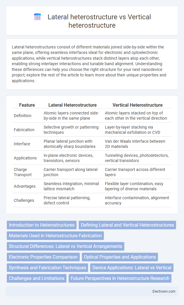
Table of Comparison
| Feature | Lateral Heterostructure | Vertical Heterostructure |
|---|---|---|
| Definition | Atomic layers connected side-by-side in the same plane | Atomic layers stacked on top of each other in the vertical direction |
| Fabrication | Selective growth or patterning techniques | Layer-by-layer stacking via mechanical exfoliation or CVD |
| Interface | Planar lateral junction with atomically sharp boundaries | Van der Waals interface between 2D materials |
| Applications | In-plane electronic devices, transistors, sensors | Tunneling devices, photodetectors, vertical transistors |
| Charge Transport | Carrier transport along lateral junction | Carrier transport across different layers |
| Advantages | Seamless integration, minimal lattice mismatch | Flexible layer combination, easy layering of diverse materials |
| Challenges | Precise lateral patterning, defect control | Interface contamination, alignment accuracy |
Introduction to Heterostructures
Heterostructures are engineered materials formed by stacking or joining different semiconductors with varying bandgaps to create unique electronic and optical properties. Lateral heterostructures seamlessly connect different materials side-by-side within the same atomic layer, enabling planar device architectures, while vertical heterostructures stack distinct layers atop one another for enhanced carrier confinement and interface quality. Your choice between lateral and vertical heterostructures impacts device performance, influencing applications in transistors, photovoltaics, and optoelectronics.
Defining Lateral and Vertical Heterostructures
Lateral heterostructures are formed by stitching different two-dimensional materials side-by-side within the same plane, creating atomically sharp interfaces along the horizontal direction. Vertical heterostructures, on the other hand, consist of stacked layers of distinct 2D materials, resulting in interfaces perpendicular to the substrate plane with strong interlayer coupling. The choice between lateral and vertical heterostructures impacts electronic, optical, and mechanical properties, making them fundamental architectures in designing van der Waals heterostructures for nanoelectronics and optoelectronics.
Materials Used in Heterostructure Fabrication
Lateral heterostructures typically involve seamless integration of two-dimensional (2D) materials such as graphene, transition metal dichalcogenides (TMDs) like MoS2 and WS2, enabling in-plane junctions with well-defined atomic interfaces. Vertical heterostructures are formed by stacking different 2D layers like graphene, hexagonal boron nitride (hBN), and TMDs, allowing precise control over interlayer coupling and electronic properties. Both fabrication methods leverage chemical vapor deposition (CVD) and mechanical exfoliation to achieve high-quality material interfaces critical for advanced nanoelectronic and optoelectronic applications.
Structural Differences: Lateral vs Vertical Arrangements
Lateral heterostructures feature side-by-side arrangements of different materials within the same plane, creating seamless boundaries along the horizontal axis. Vertical heterostructures stack different layers of materials atop one another, forming interfaces perpendicular to the substrate. Understanding these structural differences is crucial for tailoring electronic and optical properties in your device design.
Electronic Properties Comparison
Lateral heterostructures exhibit seamless in-plane junctions that enable efficient charge carrier transport with minimal scattering, resulting in high electron mobility and tunable bandgaps across the interface. Vertical heterostructures, formed by stacking different 2D materials, provide strong interlayer coupling and distinct band alignments, facilitating charge transfer and exciton dynamics beneficial for optoelectronic applications. Your choice between these heterostructures depends on the desired electronic properties such as anisotropic conductivity in lateral types or enhanced interfacial charge separation in vertical configurations.
Optical Properties and Applications
Lateral heterostructures exhibit seamless in-plane interfaces that enable efficient charge transfer and spatially confined excitons, enhancing light emission and photodetection capabilities in optoelectronic devices. Vertical heterostructures, formed by stacking atomically thin layers, promote strong interlayer coupling and tunable band gaps, which improve exciton recombination and enable applications in photovoltaics, LEDs, and tunneling transistors. Your choice between lateral and vertical heterostructures depends on the desired device architecture and specific optical performance requirements for efficient energy harvesting and photonic integration.
Synthesis and Fabrication Techniques
Lateral heterostructures are synthesized through in-plane epitaxial growth, often achieved via chemical vapor deposition (CVD) techniques that allow seamless atomic bonding between different two-dimensional materials. Vertical heterostructures, on the other hand, are typically fabricated by stacking individual monolayers using mechanical exfoliation and transfer methods or layer-by-layer growth in molecular beam epitaxy (MBE). Your choice between these heterostructure types depends on the desired interfacial properties and scalability requirements for electronic or optoelectronic device applications.
Device Applications: Lateral vs Vertical
Lateral heterostructures enable seamless in-plane integration of different materials, enhancing electronic and optoelectronic device performance such as transistors and photodetectors by allowing precise control over charge transport pathways. Vertical heterostructures offer efficient stacking of atomically thin layers, optimizing tunneling devices, light-emitting diodes, and solar cells through strong interlayer coupling and reduced interface defects. Device applications leveraging lateral heterostructures benefit from improved lateral charge carrier mobility, while vertical heterostructures excel in vertical charge transport and multi-functional device integration.
Challenges and Limitations
Lateral heterostructures face challenges in achieving precise atomic-scale control during in-plane synthesis, often resulting in defects and limited scalability. Vertical heterostructures encounter limitations related to interlayer coupling and lattice mismatch, which can degrade electronic and optical properties. Understanding these constraints is crucial for optimizing your device performance in applications like nanoelectronics and photonics.
Future Perspectives in Heterostructure Research
Future perspectives in heterostructure research emphasize the integration of lateral heterostructures for scalable, on-chip electronic and optoelectronic devices due to their atomically sharp interfaces and seamless lateral connections. Vertical heterostructures remain critical for achieving novel quantum phenomena and multifunctional device architectures by stacking diverse two-dimensional materials with precise interlayer control. Your exploration of emerging applications will benefit from understanding how combining lateral and vertical designs advances tunability, performance, and device miniaturization in next-generation nanoscale systems.
Lateral heterostructure vs Vertical heterostructure Infographic