Chemical vapor deposition (CVD) involves chemical reactions to deposit thin films on substrates, offering excellent conformality and precise control over nanoscale material properties. Physical vapor deposition (PVD), by contrast, uses physical processes like sputtering or evaporation for layer formation, often providing higher purity but less uniform coverage at the nanoscale; explore this article to understand which method suits your nanoscale material needs best.
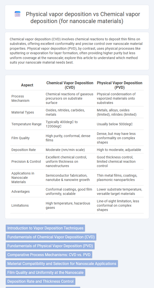
Table of Comparison
| Aspect | Chemical Vapor Deposition (CVD) | Physical Vapor Deposition (PVD) |
|---|---|---|
| Process Mechanism | Chemical reactions of gaseous precursors on substrate surface | Physical condensation of vaporized materials onto substrates |
| Material Types | Oxides, nitrides, carbides, metals | Metals, alloys, oxides (limited), nitrides (limited) |
| Temperature Range | Typically 400degC to 1200degC | Usually below 500degC |
| Film Quality | High purity, conformal, dense films | Dense, but may have less conformality on complex shapes |
| Deposition Rate | Moderate (nm/min scale) | High to moderate, adjustable |
| Precision & Control | Excellent chemical control, uniform thickness on nanostructures | Good thickness control, limited chemical reaction control |
| Applications in Nanoscale Materials | Semiconductor fabrication, nanotube & nanowire growth | Thin metal films, coatings, plasmonic nanoparticles |
| Advantages | Conformal coatings, good film uniformity, scalable | Lower substrate temperature, versatile target materials |
| Limitations | High temperature, hazardous gases | Line-of-sight limitation, less conformal on complex shapes |
Introduction to Vapor Deposition Techniques
Chemical vapor deposition (CVD) and physical vapor deposition (PVD) are two primary vapor deposition techniques used to fabricate nanoscale materials with precise control over thickness and composition. CVD involves chemical reactions of gaseous precursors on the substrate surface, enabling the growth of high-purity, conformal thin films, while PVD operates through physical processes like evaporation or sputtering, depositing material atoms or molecules onto the substrate. These techniques are fundamental in semiconductor manufacturing, nanotechnology, and coating applications due to their ability to create uniform and defect-free nanoscale layers.
Fundamentals of Chemical Vapor Deposition (CVD)
Chemical Vapor Deposition (CVD) involves chemical reactions of gaseous precursors on a heated substrate, resulting in the formation of solid nanoscale materials with precise control over composition and thickness. This process enables uniform coatings and high-purity films essential for semiconductor and nanotechnology applications. Your choice of CVD allows for superior conformality and scalability compared to Physical Vapor Deposition (PVD), especially for complex nanostructured surfaces.
Fundamentals of Physical Vapor Deposition (PVD)
Physical Vapor Deposition (PVD) involves vaporizing a solid material in a vacuum environment and condensing it onto a substrate to form thin films or nanoscale coatings. This process relies on physical methods such as evaporation, sputtering, or pulsed laser deposition to transfer atoms or molecules without chemical reactions, ensuring high purity and precise thickness control. Your nanoscale fabrication benefits from PVD's capability to produce uniform, dense layers with excellent adhesion and minimal contamination.
Comparative Process Mechanisms: CVD vs. PVD
Chemical vapor deposition (CVD) involves the chemical reaction of vapor-phase precursors on a heated substrate to form a solid nanoscale material, promoting uniform and conformal coatings. Physical vapor deposition (PVD) relies on physical processes such as sputtering or evaporation to transfer material atoms or clusters onto the substrate surface, typically producing thinner films with high purity. CVD often achieves better step coverage and complex geometries at the nanoscale, while PVD offers precise control over film thickness and composition through physical transport mechanisms.
Material Compatibility and Selection for Nanoscale Applications
Chemical vapor deposition (CVD) offers superior material compatibility for nanoscale applications by enabling the deposition of a wide range of compounds, including complex oxides and nitrides, with excellent conformality on intricate nanostructures. Physical vapor deposition (PVD) is typically limited to metals and simple alloys but provides precise control over film thickness and composition, ideal for thin metallic layers in nanoscale devices. Your choice between CVD and PVD depends on material requirements and application-specific properties such as adhesion, uniformity, and chemical composition at the nanoscale.
Film Quality and Uniformity at the Nanoscale
Chemical vapor deposition (CVD) produces films with superior conformality and compositional uniformity at the nanoscale due to its self-limiting surface reactions, enabling high-quality thin films on complex nanostructures. Physical vapor deposition (PVD) often results in less uniform films because of its line-of-sight deposition mechanism, which can create shadowing effects and non-uniform thickness on nanoscale features. CVD's ability to control film stoichiometry and density at the atomic level makes it the preferred choice for achieving precise nanoscale film quality and uniformity.
Deposition Rate and Thickness Control
Chemical vapor deposition (CVD) typically offers slower deposition rates with superior thickness uniformity, enabling precise control over nanoscale film growth through chemical reactions. Physical vapor deposition (PVD) achieves faster deposition rates but often sacrifices thickness uniformity, making it challenging to maintain consistent nanoscale film thickness across substrates. Precise thickness control in CVD is critical for functional nanoscale materials, while PVD is favored for applications requiring rapid layering despite less uniform thickness.
Industrial Applications in Nanotechnology
Chemical vapor deposition (CVD) offers precise control over film composition and thickness, making it indispensable for producing high-purity nanoscale coatings in semiconductor manufacturing and advanced electronics. Physical vapor deposition (PVD) excels in depositing thin metal and alloy films with strong adhesion, widely used in aerospace and automotive industries for wear-resistant nanoscale coatings. Your choice between CVD and PVD depends on the required material properties and application-specific performance in nanotechnology-driven industrial processes.
Challenges and Limitations of CVD and PVD
Chemical vapor deposition (CVD) faces challenges such as high processing temperatures that can limit substrate compatibility and issues with precursor toxicity and gas-phase reactions leading to unwanted by-products. Physical vapor deposition (PVD) encounters limitations including poor step coverage on complex nanostructures and difficulties in achieving uniform thickness on large-area substrates. Both techniques require precise control over process parameters to ensure reproducibility and scalability for nanoscale material applications.
Future Trends in Nanoscale Vapor Deposition
Future trends in nanoscale vapor deposition emphasize enhanced control over film uniformity and composition through atomic layer deposition techniques that build upon Chemical Vapor Deposition (CVD) and Physical Vapor Deposition (PVD) principles. The integration of in-situ monitoring and machine learning algorithms aims to optimize parameters dynamically, improving material properties at the atomic scale. Emerging hybrid processes combine CVD and PVD to exploit the advantages of both methods for fabricating multifunctional nanoscale structures with superior precision and scalability.
Chemical vapor deposition vs Physical vapor deposition (for nanoscale materials) Infographic