Optoelectronic nano devices combine optical and electronic functionalities, enabling faster data transmission and enhanced signal processing compared to pure electronic nano devices, which rely solely on electrical signals for operation. Discover how these differences impact your choice of technology by exploring the rest of the article.
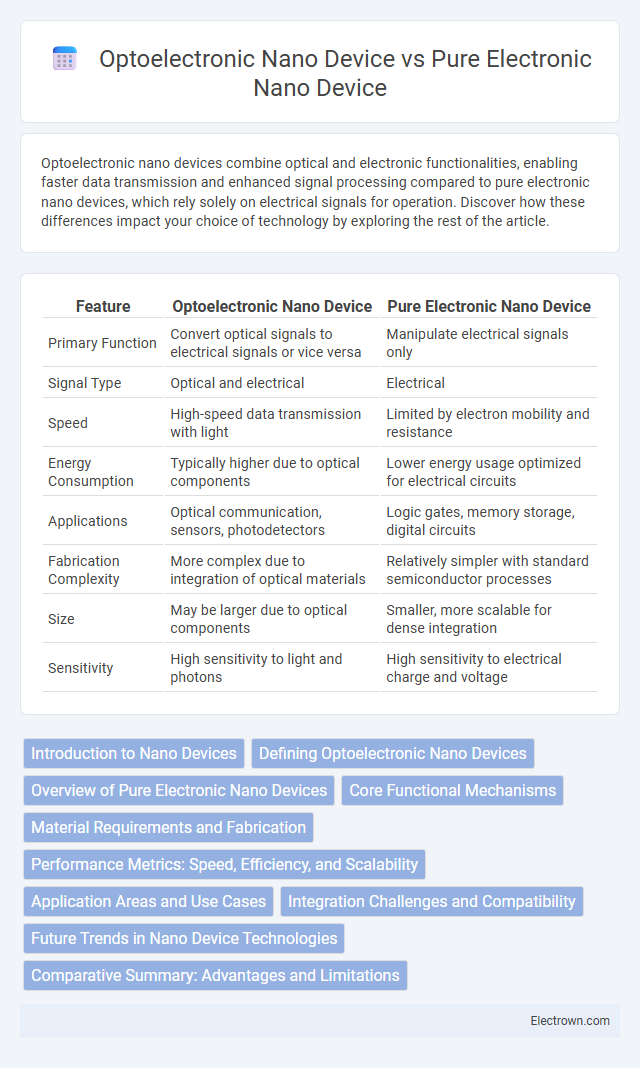
Table of Comparison
| Feature | Optoelectronic Nano Device | Pure Electronic Nano Device |
|---|---|---|
| Primary Function | Convert optical signals to electrical signals or vice versa | Manipulate electrical signals only |
| Signal Type | Optical and electrical | Electrical |
| Speed | High-speed data transmission with light | Limited by electron mobility and resistance |
| Energy Consumption | Typically higher due to optical components | Lower energy usage optimized for electrical circuits |
| Applications | Optical communication, sensors, photodetectors | Logic gates, memory storage, digital circuits |
| Fabrication Complexity | More complex due to integration of optical materials | Relatively simpler with standard semiconductor processes |
| Size | May be larger due to optical components | Smaller, more scalable for dense integration |
| Sensitivity | High sensitivity to light and photons | High sensitivity to electrical charge and voltage |
Introduction to Nano Devices
Nano devices operate at the scale of nanometers, where quantum effects significantly influence performance and functionality. Optoelectronic nano devices integrate both optical and electronic components, enabling the manipulation of light and electrons, crucial for applications in high-speed communication and sensing. Pure electronic nano devices rely solely on electron transport mechanisms for signal processing and data storage, often used in ultra-dense memory and logic circuits, making your choice dependent on the desired application and operational environment.
Defining Optoelectronic Nano Devices
Optoelectronic nano devices are nanoscale components that interact with both electrical signals and light, enabling applications like photodetectors, light-emitting diodes, and solar cells. Unlike pure electronic nano devices, which solely manipulate electrical currents for data processing or sensing, optoelectronic devices convert optical signals into electrical ones and vice versa, enhancing communication and energy efficiency. Your choice between these two depends on whether light manipulation is essential for your application's performance and functionality.
Overview of Pure Electronic Nano Devices
Pure electronic nano devices rely on the manipulation of electrons to perform functions such as switching, sensing, and data processing at the nanoscale. These devices utilize materials like silicon nanowires, carbon nanotubes, and quantum dots to achieve enhanced electrical conductivity, miniaturization, and energy efficiency. Your understanding of pure electronic nano devices is crucial for advancements in nanoelectronics, enabling faster, smaller, and more efficient electronic components.
Core Functional Mechanisms
Optoelectronic nano devices leverage the interaction between light and electrical signals, utilizing photonic properties such as photon absorption, emission, and modulation to perform functions like sensing and communication at the nanoscale. Pure electronic nano devices operate based on electron transport mechanisms, exploiting quantum tunneling, Coulomb blockade, and ballistic conduction for applications in nanoelectronics and computing. The core functional distinction lies in optoelectronic devices' reliance on photonic-electronic coupling, whereas pure electronic devices depend solely on electron charge manipulation within nanoscale materials.
Material Requirements and Fabrication
Optoelectronic nano devices require materials with strong light-matter interaction properties such as III-V semiconductors (e.g., GaAs, InP) and precise epitaxial growth techniques to achieve high quantum efficiency and optical coherence. Pure electronic nano devices rely on materials with excellent electrical conductivity and electron mobility, like silicon, graphene, or transition metal dichalcogenides, and commonly use advanced lithography and doping processes to control electronic properties at the nanoscale. Fabrication of optoelectronic devices typically involves complex strain management and surface passivation to optimize optical performance, whereas electronic nano devices focus on defect minimization and interface control to enhance charge transport and device reliability.
Performance Metrics: Speed, Efficiency, and Scalability
Optoelectronic nano devices typically offer higher speed due to faster photon-based signal transmission compared to electron-based transport in pure electronic nano devices, enhancing data processing rates. Efficiency in optoelectronic devices often surpasses pure electronic counterparts by reducing heat generation and power consumption through optical interconnects. Scalability challenges exist for both, but optoelectronic devices provide better integration potential in photonic circuits, while pure electronic nano devices benefit from mature semiconductor fabrication techniques that optimize Your system's overall performance and cost-effectiveness.
Application Areas and Use Cases
Optoelectronic nano devices are primarily utilized in advanced photonics, telecommunications, and sensing applications, including high-speed optical communication, quantum computing, and biosensing due to their ability to manipulate light at the nanoscale. Pure electronic nano devices excel in ultra-low power electronics, nano-transistors, and memory storage, driving innovations in high-performance computing, flexible electronics, and nanoscale sensors. Your choice depends on whether your focus lies in light-based signal processing and detection (optoelectronic) or purely electronic charge manipulation for computing and storage (pure electronic).
Integration Challenges and Compatibility
Optoelectronic nano devices face integration challenges due to material heterogeneity and the need for precise alignment between optical and electronic components, which complicates compatibility with traditional semiconductor fabrication processes. Pure electronic nano devices benefit from established CMOS compatibility, enabling easier integration into existing electronic circuits but lack the multifunctional capabilities of optoelectronic systems. Your choice depends on balancing these integration complexities with the desired device performance and system compatibility.
Future Trends in Nano Device Technologies
Future trends in nano device technologies emphasize the integration of optoelectronic nano devices with pure electronic nano devices to enhance speed, efficiency, and functionality. Optoelectronic nano devices leverage photon-electron interactions for high-speed data transmission and low energy consumption, making them crucial for next-generation communication systems and quantum computing. Your applications will benefit from hybrid nanosystems that combine the processing power of electronic devices with the high-bandwidth capabilities of optoelectronics, driving innovation in AI, IoT, and 5G/6G networks.
Comparative Summary: Advantages and Limitations
Optoelectronic nano devices offer faster data transmission speeds and higher bandwidth by utilizing photons, making them ideal for high-speed communication applications, but they face challenges in integration complexity and power consumption. Pure electronic nano devices provide superior scalability, lower fabrication costs, and easier integration with existing semiconductor technology, yet they are limited by slower signal processing speeds and increased heat generation. The choice between the two depends on specific application requirements such as speed, power efficiency, and integration constraints.
Optoelectronic Nano Device vs Pure Electronic Nano Device Infographic