Electron localization in nanostructures confines charge carriers to specific regions, influencing electronic and optical properties, while delocalization allows electrons to move freely across the structure, enhancing conductivity and interaction strength. Understanding how electron behavior shifts between these states can optimize your design of nanoscale devices; explore the rest of the article to learn more about these critical phenomena.
Table of Comparison
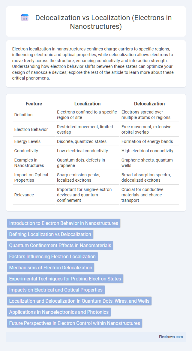
| Feature | Localization | Delocalization |
|---|---|---|
| Definition | Electrons confined to a specific region or site | Electrons spread over multiple atoms or regions |
| Electron Behavior | Restricted movement, limited overlap | Free movement, extensive orbital overlap |
| Energy Levels | Discrete, quantized states | Formation of energy bands |
| Conductivity | Low electrical conductivity | High electrical conductivity |
| Examples in Nanostructures | Quantum dots, defects in graphene | Graphene sheets, quantum wells |
| Impact on Optical Properties | Sharp emission peaks, localized excitons | Broad absorption spectra, delocalized excitons |
| Relevance | Important for single-electron devices and quantum confinement | Crucial for conductive materials and charge transport |
Introduction to Electron Behavior in Nanostructures
Electron behavior in nanostructures is governed by quantum confinement effects that significantly impact their localization and delocalization properties. Localization occurs when electrons are confined to specific regions due to defects or spatial constraints, influencing electronic transport and optical properties. Delocalization, in contrast, enables electrons to spread across extended states, enhancing conductivity and enabling phenomena such as quantum tunneling and coherent transport in nanoscale materials.
Defining Localization vs Delocalization
Localization in nanostructures refers to electrons confined within a limited spatial region due to defects, impurities, or strong electron interactions, leading to discrete energy states and reduced conductivity. Delocalization occurs when electrons are spread over extended regions or entire nanostructures, enabling coherent quantum states and enhanced charge transport. The degree of localization or delocalization critically influences the electronic, optical, and transport properties of nanoscale materials.
Quantum Confinement Effects in Nanomaterials
Quantum confinement effects in nanomaterials drastically influence electron localization by restricting electron motion within dimensions comparable to the electron's de Broglie wavelength. These effects cause discrete energy levels instead of continuous bands, enhancing electron localization and altering optical and electronic properties. The balance between localization and delocalization determines the functionality of nanostructured devices such as quantum dots and nanowires.
Factors Influencing Electron Localization
Electron localization in nanostructures is strongly influenced by factors such as structural disorder, quantum confinement, and electron-electron interactions. Variations in atomic arrangement or defects create potential fluctuations that trap electrons, while reduced dimensionality in quantum dots enhances localization by restricting electron motion. Your ability to control these parameters enables tailoring electronic properties for applications like quantum computing and nanoscale electronics.
Mechanisms of Electron Delocalization
Electron delocalization in nanostructures primarily occurs through quantum tunneling and wavefunction overlap between adjacent atomic or molecular orbitals, enabling charge carriers to spread over multiple sites. Coupling strength, energy level alignment, and the spatial arrangement of nanoparticles or molecular units critically influence the degree of delocalization. Coherent electron transport and hybridization of electronic states further enhance delocalization, facilitating conductivity and unique optoelectronic properties in nanoscale systems.
Experimental Techniques for Probing Electron States
Scanning tunneling microscopy (STM) and angle-resolved photoemission spectroscopy (ARPES) are key experimental techniques for probing electron localization and delocalization in nanostructures. STM provides real-space imaging of localized electron states with atomic resolution, while ARPES offers momentum-space information, revealing electron band structures and delocalized states. Understanding these measurements helps you analyze electron behavior critical for designing nanoscale electronic devices.
Impacts on Electrical and Optical Properties
Localization of electrons in nanostructures leads to discrete energy levels, significantly enhancing optical properties like photoluminescence and enabling sharp spectral features. Delocalization facilitates electron mobility, resulting in higher electrical conductivity and improved charge transport efficiency. Understanding your nanostructure's electron behavior helps tailor its performance in applications such as quantum dots, sensors, and optoelectronic devices.
Localization and Delocalization in Quantum Dots, Wires, and Wells
In nanostructures such as quantum dots, wires, and wells, electron localization refers to electrons being confined within a small spatial region, resulting in discrete energy levels and enhanced quantum effects. Delocalization occurs when electrons can move freely across larger areas, like in quantum wires or wells, leading to continuous energy bands and altered electronic properties. Your ability to manipulate these localization phenomena is crucial for tailoring the optical and electrical behavior of nanoscale devices.
Applications in Nanoelectronics and Photonics
Localization of electrons in nanostructures enhances charge confinement, critical for quantum dot-based single-electron transistors and memory devices, enabling precise control over electronic states. Delocalization facilitates electron mobility across nanowires and graphene sheets, boosting conductivity and enabling efficient light-matter interactions essential for photonic devices like nanoscale lasers and photodetectors. Tailoring the balance between localized and delocalized electronic states optimizes performance in nanoelectronics and photonics by modulating charge transport, optical absorption, and emission properties.
Future Perspectives in Electron Control within Nanostructures
Future perspectives in electron control within nanostructures emphasize advancements in manipulating electron localization and delocalization to enhance quantum computing, nanoelectronics, and energy-efficient devices. Emerging techniques in precise tuning of potential wells and barriers allow your ability to control electron wavefunctions at the nanoscale, facilitating improved coherence times and electron mobility. Integration of novel materials, such as topological insulators and two-dimensional semiconductors, promises to revolutionize electron dynamics through tailored localization-delocalization transitions.
Localization vs Delocalization (electrons in nanostructures) Infographic