Ion implantation precisely introduces dopants into a semiconductor by accelerating ions into the substrate, offering controlled depth and concentration but may cause lattice damage requiring annealing. Diffusion doping relies on thermal processes to drive dopants into the material, providing gradual penetration but less precise control over profiles. Explore the rest of the article to understand which technique best suits your semiconductor fabrication needs.
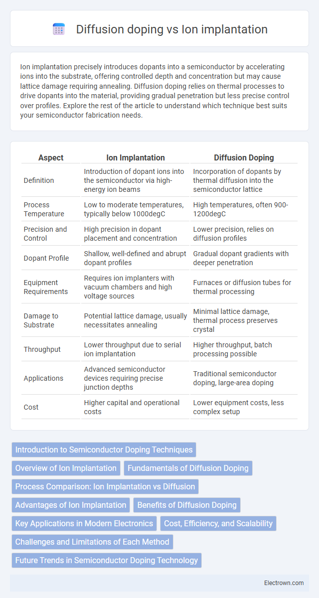
Table of Comparison
| Aspect | Ion Implantation | Diffusion Doping |
|---|---|---|
| Definition | Introduction of dopant ions into the semiconductor via high-energy ion beams | Incorporation of dopants by thermal diffusion into the semiconductor lattice |
| Process Temperature | Low to moderate temperatures, typically below 1000degC | High temperatures, often 900-1200degC |
| Precision and Control | High precision in dopant placement and concentration | Lower precision, relies on diffusion profiles |
| Dopant Profile | Shallow, well-defined and abrupt dopant profiles | Gradual dopant gradients with deeper penetration |
| Equipment Requirements | Requires ion implanters with vacuum chambers and high voltage sources | Furnaces or diffusion tubes for thermal processing |
| Damage to Substrate | Potential lattice damage, usually necessitates annealing | Minimal lattice damage, thermal process preserves crystal |
| Throughput | Lower throughput due to serial ion implantation | Higher throughput, batch processing possible |
| Applications | Advanced semiconductor devices requiring precise junction depths | Traditional semiconductor doping, large-area doping |
| Cost | Higher capital and operational costs | Lower equipment costs, less complex setup |
Introduction to Semiconductor Doping Techniques
Ion implantation offers precise control over dopant concentration and depth by accelerating ions directly into the semiconductor substrate, enabling high accuracy and minimal thermal budget. Diffusion doping relies on thermal processes where dopants diffuse into the semiconductor at elevated temperatures, leading to less control over profile precision and potential wafer deformation. Your choice between these techniques depends on device specifications, manufacturing constraints, and desired electrical characteristics.
Overview of Ion Implantation
Ion implantation is a precise semiconductor doping technique where ions are accelerated and embedded into a substrate, enabling controlled modification of electrical properties at specific depths. Unlike diffusion doping, which relies on temperature-driven dopant movement, ion implantation offers superior accuracy in dose, depth, and lateral distribution, critical for advanced integrated circuit fabrication. Your semiconductor devices benefit from enhanced performance and reliability through this method's ability to introduce dopants with minimal thermal budget impact.
Fundamentals of Diffusion Doping
Diffusion doping involves the introduction of dopant atoms into a semiconductor substrate by exposing it to a high-temperature environment where atoms diffuse into the material based on concentration gradients and temperature-driven atomic mobility. The process controls dopant depth and concentration profiles through variables such as temperature, time, and ambient gas composition, enabling precise tailoring of semiconductor electrical properties. Your semiconductor device's performance relies on optimizing diffusion parameters to achieve uniform dopant distribution and desired junction depths.
Process Comparison: Ion Implantation vs Diffusion
Ion implantation involves accelerating ions into a semiconductor substrate, enabling precise control of dopant concentration and depth profiles, while diffusion doping relies on thermal processes to introduce dopants by diffusion from a gas or solid source. Ion implantation offers superior spatial accuracy and less thermal budget impact compared to diffusion, which requires high temperatures for extended times, potentially causing unwanted diffusion and contamination. The process choice impacts semiconductor device performance, with ion implantation preferred for modern integrated circuits due to its scalability and minimal substrate damage.
Advantages of Ion Implantation
Ion implantation offers precise control over dopant concentration and depth profiles, enabling accurate tailoring of semiconductor device characteristics. This technique provides excellent uniformity and reproducibility, minimizing contamination risks often associated with diffusion doping. High-energy ion beams allow for doping at lower temperatures, reducing thermal budget and preventing unwanted diffusion or damage to sensitive device structures.
Benefits of Diffusion Doping
Diffusion doping offers benefits such as uniform dopant distribution and simpler equipment requirements compared to ion implantation. This method enables the formation of shallow junctions with minimal crystal damage, preserving the substrate's integrity. Your semiconductor fabrication process can benefit from cost-effective scalability and enhanced thermal stability through diffusion doping.
Key Applications in Modern Electronics
Ion implantation is widely utilized in modern electronics for precise doping of semiconductor wafers, enabling the fabrication of integrated circuits with nanoscale features essential for advanced microprocessors and memory devices. Diffusion doping remains valuable for creating uniform dopant distributions in power devices and sensors due to its cost-effectiveness and simplicity in large-scale production. Your choice between ion implantation and diffusion doping depends on the required precision, device architecture, and performance specifications within semiconductor manufacturing.
Cost, Efficiency, and Scalability
Ion implantation offers higher precision and efficiency in doping semiconductor materials, enabling controlled ion placement at specific depths, which reduces material waste and enhances device performance compared to diffusion doping. While ion implantation equipment incurs higher initial costs, its scalability supports mass production with consistent doping profiles, lowering per-unit expenses over time. Diffusion doping remains less expensive upfront but exhibits lower efficiency and limited scalability due to reliance on high-temperature processing and less precise dopant control.
Challenges and Limitations of Each Method
Ion implantation faces challenges such as lattice damage and channeling effects, which can reduce doping uniformity and require post-implantation annealing to restore crystal structure. Diffusion doping is limited by slower doping profiles and less precise control over dopant depth and concentration, making it less suitable for advanced, ultra-shallow junctions. Both methods struggle with maintaining dopant activation and minimizing defects, impacting device performance and scalability in semiconductor fabrication.
Future Trends in Semiconductor Doping Technology
Ion implantation demonstrates increasing precision and scalability for advanced semiconductor doping, enabling ultra-shallow junctions crucial for next-generation transistors. Emerging trends emphasize plasma doping and advanced annealing techniques to minimize lattice damage while enhancing dopant activation. Diffusion doping, while still valuable for specific applications, faces limitations in uniformity and spatial control compared to ion implantation in future high-performance semiconductor manufacturing.
Ion implantation vs Diffusion doping Infographic